


436
CHAPTER 19 SERIAL INTERFACE CHANNEL 1
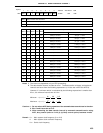
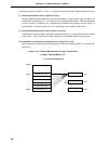
Cautions 1. Because, in the basic transmission/reception mode, the automatic transmit/receive
function writes/reads data to/from the buffer RAM after 1-byte transmission/reception,
an interval is inserted till the next transmission/reception. As the buffer RAM write/
read is performed at the same time as CPU processing, the maximum interval is
dependent upon CPU processing and the value of the automatic data transmit/
receive interval specify register (ADTI) (see (5) Automatic transmit/receive interval
time).
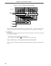
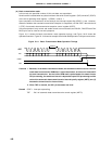
2. When TRF is cleared, the SO1 pin becomes low level.
Remark CSIIF0 : Interrupt request flag
TRF : Bit 3 of automatic data transmit/receive control register (ADTC)
SCK1
SO1 D7 D6 D5 D4 D3 D2 D1 D0 D7 D6 D5 D4 D3 D2 D1 D0
CSIIF1
TRF
SI1 D7D6D5D4D3D2D1D0 D7D6D5D4D3D2D1D0
Interval
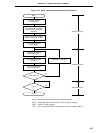
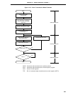
(3) Communication operation
(a) Basic transmission/reception mode
This transmission/reception mode is the same as the 3-wire serial I/O mode in which specified number
of data are transmitted/received in 8-bit units.
Serial transfer is started when any data is written to the serial I/O shift register 1 (SIO1) while bit 7 (CSIE1)
of the serial operating mode register 1 (CSIM1) is set to 1.
Upon completion of transmission of the last byte, the interrupt request flag (CSIIF1) is set. However,
determine whether the automatic transmission/reception is completed, not with CSIIF1 but with bit 3
(TRF) of the automatic data transmission/reception control register (ADTC).
If busy control and strobe control are not executed, the P23/STB and P24/BUSY pins can be used as
normal input/output ports.
Figure 19-8 shows the basic transmission/reception mode operation timings, and Figure 19-9 shows
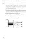
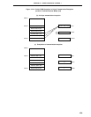
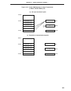
the operation flowchart. Figure 19-10 shows an example of the buffer RAM operation in 6-byte
transmission/reception.
Figure 19-8. Basic Transmission/Reception Mode Operation Timings