


455
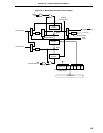
CHAPTER 19 SERIAL INTERFACE CHANNEL 1
(a) When the automatic transmit/receive function is used by the internal clock
If bit 1 (CSIM11) of serial operation mode register 1 (CSIM1) is set at (1), the internal clock operates.
If the automatic transmit/receive function is operated by the internal clock, interval timing by CPU
processing is as follows.
When bit 7 (ADTI7) of automatic data transmit/receive interval specify register (ADTI) is set to 0, the
interval depends on the CPU processing. When ADTI7 is set to 1, it depends on the contents of the
ADTI or CPU processing, whichever is greater.
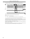
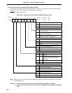
Refer to Figure 19-5. Automatic Data Transmit/Receive Interval Specify Register Format for the
intervals which are set by the ADTI.
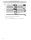
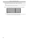
Table 19-2. Interval Timing through CPU Processing (when the Internal Clock is Operating)
CPU Processing Interval Time
When using multiplication instruction Max. (2.5TSCK, 13TCPU)
When using division instruction Max. (2.5TSCK, 20TCPU)
External access 1 wait mode Max. (2.5TSCK, 9TCPU)
Other than above Max. (2.5T
SCK, 7TCPU)
TSCK : 1/fSCK
fSCK : Serial clock frequency
TCPU : 1/fCPU
fCPU : CPU clock (set by bits 0 to 2 (PCC0 to PCC2) of the processor clock control register (PCC)
and bit 0 (MCS) of the oscillation mode selection register (OSMS))
MAX. (a, b) : a or b, whichever is greater
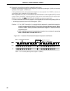
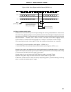
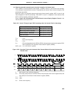
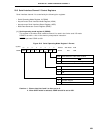
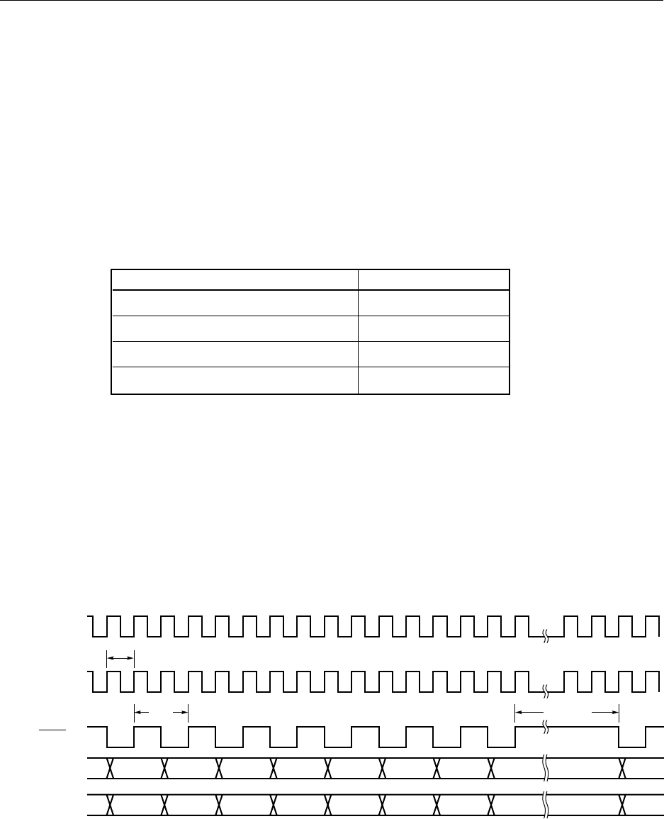
Figure 19-24. Operation Timing with Automatic Data Transmit/Receive Function Performed by
Internal Clock
f
X : Main system clock oscillation frequency
f
CPU : CPU clock (set by bits 0 to 2 (PCC0 to PCC2) of the processor clock control register (PCC) and
bit 0 (MCS) of the oscillation mode selection register (OSMS).
TCPU : 1/fCPU
TSCK : 1/fSCK
fSCK : Serial clock frequency
f
X
f
CPU
SCK1
SO1
SI1
T
CPU
T
SCK
D7 D6 D5 D4 D3 D2 D1 D0
D7 D6 D5 D4 D3 D2 D1 D0
Interval