


429
CHAPTER 19 SERIAL INTERFACE CHANNEL 1
19.4.3 3-wire serial I/O mode operation with automatic transmit/receive function
This 3-wire serial I/O mode is used for transmission/reception of a maximum of 32-byte data without the use of
software. Once transfer is started, the data prestored in the RAM can be transmitted by the set number of bytes,
and data can be received and stored in the RAM by the set number of bytes.
Handshake signals (STB and BUSY) are supported by hardware to transmit/receive data continuously. OSD
(On Screen Display) LSI and peripheral LSI including LCD controller/driver can be connected without difficulty.
(1) Register setting
The 3-wire serial I/O mode with automatic transmit/receive function is set with the serial operating mode
register 1 (CSIM1), the automatic data transmit/receive control register (ADTC) and the automatic data
transmit/receive interval specify register (ADTI).
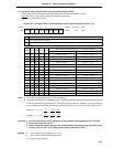
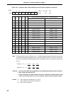
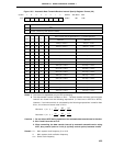
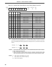
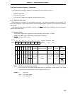
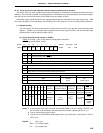
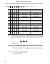
(a) Serial operating mode register 1 (CSIM1)
CSIM1 is set with a 1-bit or 8-bit memory manipulation instruction.
RESET input sets CSIM1 to 00H.
Notes 1. If the external clock input has been selected with CSIM11 set to 0, set bit 1 (BUSY1) and
bit 2 (STRB) of the automatic data transmit/receive control register (ADTC) to 0, 0.
2. Can be used freely as port function.
3. Can be used as P20 (CMOS input/output) when only transmitter is used (set bit 7 (RE) of
ADTC to 0).
Remark x : Don’t care
PMxx : Port mode register
Pxx : Port output latch
Operation
enable
6<5>43210<7>
Symbol
CSIM1 CSIE1 DIR ATE 0 0 0
CSIM11 CSIM10
CSIM11
0
1
Serial Interface Channel 1 Clock Selection
Clock externally input to SCK1 pin
Note 1
8-bit timer register 2 (TM2) output
SCK1
(Input)
1 Clock specified with bits 4 to 7 of timer clock select register 3 (TCL3)
CSIE
1
0
CSIM10
x
0
1
FF68H 00H R/W
Address After Reset R/W
CSIM
11
P20 PM21 P21 PM22
Shift Register 1
Operation
Serial Clock Counter
Operation Control
SI1/P20 Pin
Function
SCK1/P22
Pin Function
x
1
0
1
0
x00
1x
1
Note 2 Note 2
Note 2 Note 2
Count
operation
SI1
Note 3
(Input)
xxxxx
Operation
stop
Clear
P20 (CMOS
input/output)
P22 (CMOS
input/output)
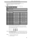
ATE
0
Serial Interface Channel 1 Operating Mode Selection
3-wire serial I/O mode
DIR
0
1
Start Bit
MSB
LSB
SI1 Pin Function
SI1/P20
(Input)
SO1 Pin Function
SO1
(CMOS output)
x
PM20
SO1/P21 Pin
Function
SO1 (CMOS
output)
P21 (CMOS
input/output)
SCK1
(CMOS
output)
1
Note 2
Note 2
Note 3Note 3
P22
1 3-wire serial I/O mode with automatic transmit/receive function