


399
CHAPTER 18 SERIAL INTERFACE CHANNEL 0 (
µ
PD78078Y Subseries)
V
DD
V
DD
SCL
SDA0(SDA1)
Master device
Clock output
(Clock input)
Data output
Data input
Slave devices
(Clock output)
Clock input
Data output
Data input
SCL
SDA0(SDA1)
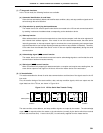
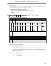
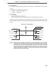
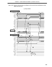
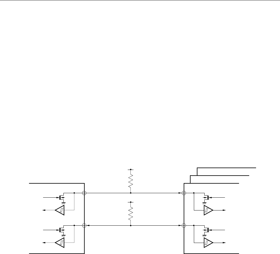
(5) Pin configurations
The configurations of the serial clock pin SCL and the serial data bus pins SDA0 (SDA1) are shown below.
(a) SCL
Pin for serial clock input/output dual-function pin.
<1> Master .... N-ch open-drain output
<2> Slave ...... Schmitt input
(b) SDA0 (SDA1)
Serial data input/output dual-function pin.
Uses N-ch open-drain output and Schmitt-input buffers for both master and slave devices.
Note that pull-up resistors are required to connect to both serial clock line and serial data bus line, because
open-drain buffers are used for the serial clock pin (SCL) and the serial data bus pin (SDA0 or SDA1) on the
I
2
C bus.
Figure 18-21. Pin Configuration
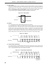
Caution Because the N-ch open-drain output must be in the high-impedance state during data
reception, set bit 7 (BSYE) of the serial bus interface control register (SBIC) to 1 before
writing FFH to the serial I/O shift register 0 (SIO0). However, do not write FFH to the SIO0
during data reception when using the wake-up function (when bit 5 (WUP) of the serial
operation mode register 0 (CSIM0)). N-ch open-drain always enters the high-impedance
state even if FFH is not written to SIO0.