


192
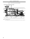
CHAPTER 8 16-BIT TIMER/EVENT COUNTER
Remarks 1. fXX : Main system clock frequency (fX or fX/2)
2. fX : Main system clock oscillation frequency
3. f
XT : Subsystem clock oscillation frequency
4. TI00 : 16-bit timer/event counter input pin
5. TM0 : 16-bit timer register
6. MCS : Bit 0 of oscillation mode selection register (OSMS)
7. Figures in parentheses apply to operation with f
X = 5.0 MHz or fXT = 32.768 kHz.
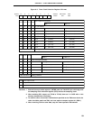
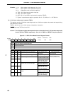
(2) 16-bit timer mode control register (TMC0)
This register sets the 16-bit timer operating mode, the 16-bit timer register clear mode and output timing,
and detects an overflow.
TMC0 is set with a 1-bit or 8-bit memory manipulation instruction.
RESET input sets TMC0 value to 00H.
Caution The 16-bit timer register starts operation when a value other than 0, 0, 0 (operation stop mode)
is set in TMC01 to TMC03, respectively. Set 0, 0, 0 in TMC01 to TMC03 to stop the operation.
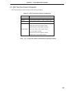
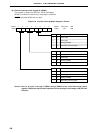
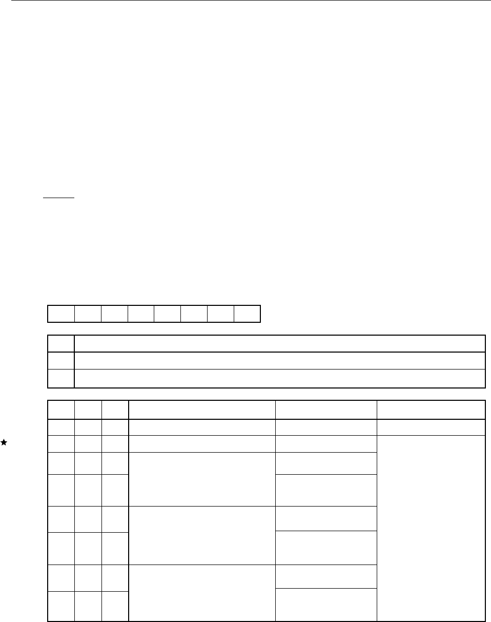
Figure 8-4. 16-Bit Timer Mode Control Register Format
0000
TMC03 TMC02 TMC01
OVF0
7654321<0>Symbol
TMC0
FF48H 00H R/W
Address After Reset R/W
OVF0 16-Bit Timer Register Overflow Detection
0 Overflow not detected
1 Overflow detected
TMC03 TMC02 TMC01
Operating Mode and Clear Mode TO0 Output Timing Interrupt Generation
000
Operation stop (TM0 cleared to 0)
No change
Not Generated
001
PWM mode
(free running)
PWM pulse output
010
011
100
101
110
111
Free running mode
TM0 and CR00 match,
or TM0 and CR01 match.
TM0 and CR00 match,
TM0 and CR01 match,
or on TI00 valid edge.
TM0 and CR00 match,
or TM0 and CR01 match.
TM0 and CR00 match,
TM0 and CR01 match,
or on TI00 valid edge
TM0 and CR00 match,
or TM0 and CR01 match.
TM0 and CR00 match,
TM0 and CR01 match,
or on TI00 valid edge
Clear & start on TI00 valid edge
Clear & start when TM0 and CR00
match
Generated when
TM0 and CR00 match,
or TM0 and CR01 match.