


539
CHAPTER 23 EXTERNAL DEVICE EXPANSION FUNCTION
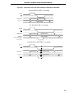
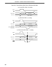
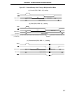
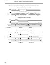
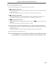
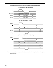
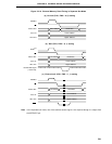
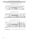
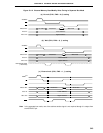
23.3.2 Timings in separate bus mode
Timing control signal output pins in the separate bus mode are as follows.
(1) RD pin (Alternate function: P64)
Read strobe signal output pin. The read strobe signal is output in data accesses and instruction fetches
from external memory.
During internal memory access, the read strobe signal is not output (maintains high level).
(2) WR pin (Alternate function: P65)
Write strobe signal output pin. The write strobe signal is output in data access to external memory.
During internal memory access, the write strobe signal is not output (maintains high level).
(3) WAIT pin (Alternate function: P66)
External wait signal input pin. When the external wait is not used, the WAIT pin can be used as an input/
output port.
During internal memory access, the external wait signal is ignored.
(4) AD0 to AD7, A0 to A7, A8 to A15 pins (Alternate function : P40 to P47, P80 to P87, P50 to P57)
Address/data signal output pin. Valid signal is output or input during data accesses and instruction fetches
from external memory.
These signals change when the internal memory is accessed (output values are undefined).
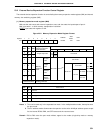
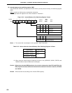
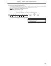
Timing charts are shown in Figure 23-9 to 23-12.
Caution In the separate bus mode, use of the address strobe signal is not required though it is output
from the ASTB/P67 pin. The output timings of the signals are shown in Figure 23-9 to 23-12.