


589
CHAPTER 28 INSTRUCTION SET
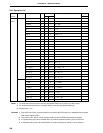
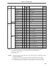
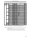
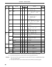
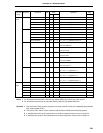
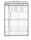
Instruction Mnemonic Operands Byte Clock Operation Flag
Group
Note 1 Note 2
ZACCY
Bit mani- AND1 CY, saddr.bit 3 6 7 CY ← CY /\ (saddr.bit) x
pulation CY, sfr.bit 3 — 7 CY ← CY /\ sfr.bit x
CY, A.bit 2 4 — CY ← CY /\ A.bit x
CY, PSW.bit 3 — 7 CY ← CY /\ PSW.bit x
CY, [HL].bit 2 6 7 + n CY ← CY /\ (HL).bit x
OR1 CY, saddr.bit 3 6 7 CY ← CY \/ (saddr.bit) x
CY, sfr.bit 3 — 7 CY ← CY \/ sfr.bit x
CY, A.bit 2 4 — CY ← CY \/ A.bit x
CY, PSW.bit 3 — 7 CY ← CY \/ PSW.bit x
CY, [HL].bit 2 6 7 + n CY ← CY \/ (HL).bit x
XOR1 CY, saddr.bit 3 6 7 CY ← CY \/ (saddr.bit) x
CY, sfr.bit 3 — 7 CY ← CY \/ sfr.bit x
CY, A.bit 2 4 — CY ← CY \/ A.bit x
CY, PSW. bit 3 — 7 CY ← CY \/ PSW.bit x
CY, [HL].bit 2 6 7 + n CY ← CY \/ (HL).bit x
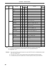
SET1 saddr.bit 2 4 6 (saddr.bit) ← 1
sfr.bit 3 — 8 sfr.bit ← 1
A.bit 2 4 — A.bit ← 1
PSW.bit 2 — 6 PSW.bit ← 1xxx
[HL].bit 2 6 8+n+m (HL).bit ← 1
CLR1 saddr.bit 2 4 6 (saddr.bit) ← 0
sfr.bit 3 — 8 sfr.bit ← 0
A.bit 2 4 — A.bit ← 0
PSW.bit 2 — 6 PSW.bit ← 0xxx
[HL].bit 2 6 8+n+m (HL).bit ← 0
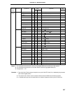
SET1 CY 1 2 — CY ← 11
CLR1 CY 1 2 — CY ← 00
NOT1 CY 1 2 — CY ← CY x
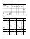
Notes 1. For instructions that access the internal high-speed RAM area or perform no data access
2. For instructions that access an area other than the internal high-speed RAM area
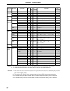
Remarks 1. One clock in the “Clock” columns is equal to one cycle of the CPU clock (f
CPU) selected by the processor
clock control register (PCC).
2. The values in the “Clock” column assumes that the internal ROM area contains programs.
3. n indicates wait cycles to be inserted when an external expansion memory area is read from.
4. m indicates wait cycles to be inserted when an external expansion memory area is written to.