


413
CHAPTER 18 SERIAL INTERFACE CHANNEL 0 (
µ
PD78078Y Subseries)
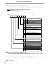
18.4.7 SCK0/SCL/P27 pin output manipulation
The SCK0/SCL/P27 pin enables static output by manipulating software in addition to normal serial clock output.
The value of serial clocks can be set by software (SI0/SB0/SDA0 and SO0/SB1/SDA1 pins are controlled with the
RELT and CMDT bits of serial bus interface control register (SBIC)).
The SCK0/SCL/P27 pin output should be manipulated as described below.
(1) In 3-wire serial I/O mode and 2-wire serial I/O mode
The SCK0/SCL/P27 pin output level is manipulated by the P27 output latch.
<1> Set serial operating mode register 0 (CSIM0) (SCK0 pin is set in the output mode and serial operation
is enabled). While serial transfer is suspended, SCK0 is set to 1.
<2> Manipulate the content of the P27 output latch by executing the bit manipulation instruction.
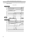
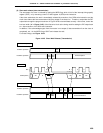
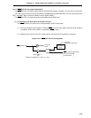
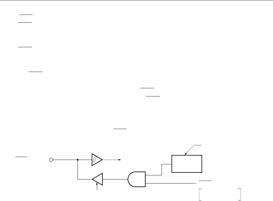
Figure 18-27. SCK0/SCL/P27 Pin Configuration
To Internal
Circuit
SCK0/SCL/P27
P27 Output
Latch
When CSIE0 = 1
and
CSIM01 and CSIM00 are 1 and 0, or 1 and 1.
SCK0 (1 when transfer stops)
From Serial Clock
Control Circuit
Set by bit
manipulation instruction