5-30 Operating Registers
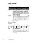
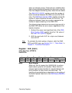
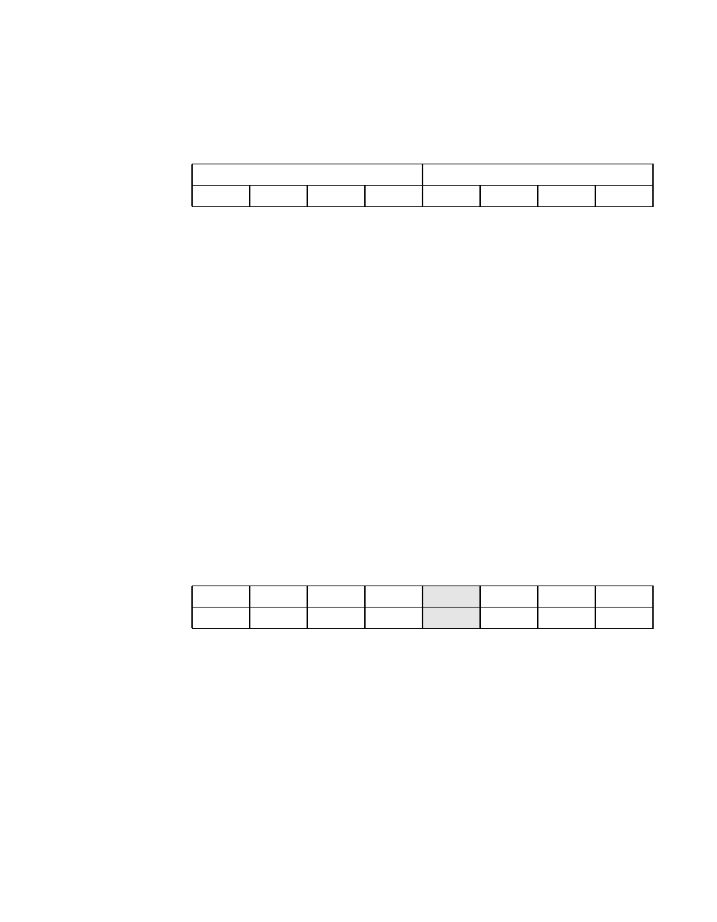
Register: 0x19 (0x99)
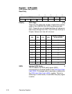
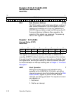
Chip Test One (CTEST1)
Read Only
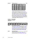
FMT[3:0] Byte Empty in DMA FIFO [7:4]
These bits identify the bottom bytes in the DMA FIFO that
are empty. Each bit corresponds to a byte lane in the
DMA FIFO. For example, if byte lane three is empty, then
FMT3 will be set. Since the FMT flags indicate the status
of bytes at the bottom of the FIFO, if all FMT bits are set,
the DMA FIFO is empty.
FFL[3:0] Byte Full in DMA FIFO [3:0]
These status bits identify the top bytes in the DMA FIFO
that are full. Each bit corresponds to a byte lane in the
DMA FIFO. For example, if byte lane three is full then
FFL3 is set. Since the FFL flags indicate the status of
bytes at the top of the FIFO, if all FFL bits are set, the
DMA FIFO is full.
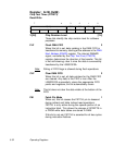
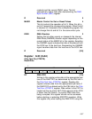
Register: 0x1A (0x9A)
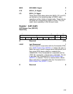
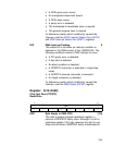
Chip Test Two (CTEST2)
Read Only
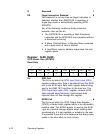
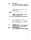
DDIR Data Transfer Direction 7
This status bit indicates which direction data is being
transferred. When this bit is set, the data will be
transferred from the SCSI bus to the host bus. When this
bit is clear, the data is transferred from the host bus to
the SCSI bus.
7430
FMT[3:0] FFL[3:0]
11110000
76543210
DDIR SIGP CIO CM R TEOP DREQ DACK
00xx0001


