3-2 PCI Functional Description
The LSI53C810A operating registers are available in both the upper and
lower 128-byte portions of the 256-byte space selected.
At initialization time, each PCI device is assigned a base address for
memory and I/O accesses. In the case of the LSI53C810A, the upper
24 bits of the address are selected. On every access, the LSI53C810A
compares its assigned base addresses with the value on the
Address/Data bus during the PCI address phase. If the upper 24 bits
match, the access is for the LSI53C810A and the low-order eight bits
define the register being accessed. A decode of C_BE/[3:0] determines
which registers and what type of access is to be performed.
I/O Space – The PCI specification defines I/O space as a contiguous
32-bit I/O address that is shared by all system resources, including the
LSI53C810A. Base Address Zero (I/O) determines which 256-byte I/O
area this device occupies.
Memory Space – The PCI specification defines memory space as a
contiguous 32-bit memory address that is shared by all system
resources, including the LSI53C810A. Base Address One (Memory)
determines which 256-byte memory area this device occupies.
3.1.2 PCI Bus Commands and Functions Supported
Bus commands indicate to the target the type of transaction the master
is requesting. Bus commands are encoded on the C_BE/[3:0] lines
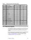
during the address phase. PCI bus commands and encoding types
appear in Table 3.1.
3.1.2.1 I/O Read Command
The I/O Read command reads data from an agent mapped in I/O
address space. All 32 address bits are decoded.
3.1.2.2 I/O Write Command
The I/O Write command writes data to an agent when mapped in I/O
address space. All 32 address bits are decoded.


