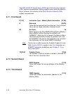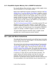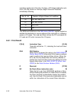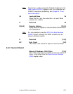
6-42 Instruction Set of the I/O Processor
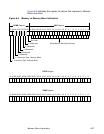
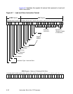
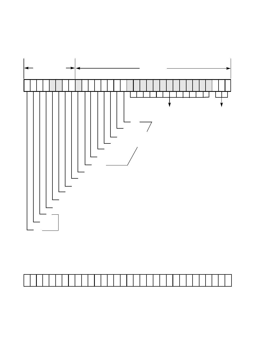
Figure 6.7 illustrates the register bit values that represent a Load and
Store instruction.
Figure 6.7 Load and Store Instruction Format
31 30
29 28 27 26 25 24 23 22 21 20 19 18 17 16 15 14 13 12 11 10 9 8 7 6 5 4 3 2 1
0
31 30
29 28 27 26 25 24 23 22 21 20 19 18 17 16 15 14 13 12 11 10 9 8 7 6 5 4 3 2 1
0
DSPS Register - Memory/ I/O Address/DSA Offset
DCMD Register DBC Register
A0
A1
A2
A3
A4
A5
A6
0 (Reserved)
Load/Store
No Flush
0 - Reserved
0 - Reserved
DSA Relative
1
1
1
Register
Address
Instruction Type - Load and Store
Reserved
(must be 0)
Byte Count
(Number of bytes
to load/store)


