


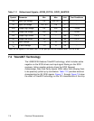
7-10 Electrical Characteristics
7.3 AC Characteristics
The AC characteristics described in this section apply over the entire
range of operating conditions (refer to Section 7.1, “DC Characteristics”).
Chip timings are based on simulation at worst case voltage, temperature,
and processing. Timings were developed with a load capacitance of
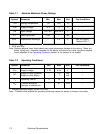
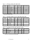
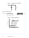
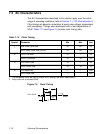
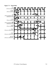
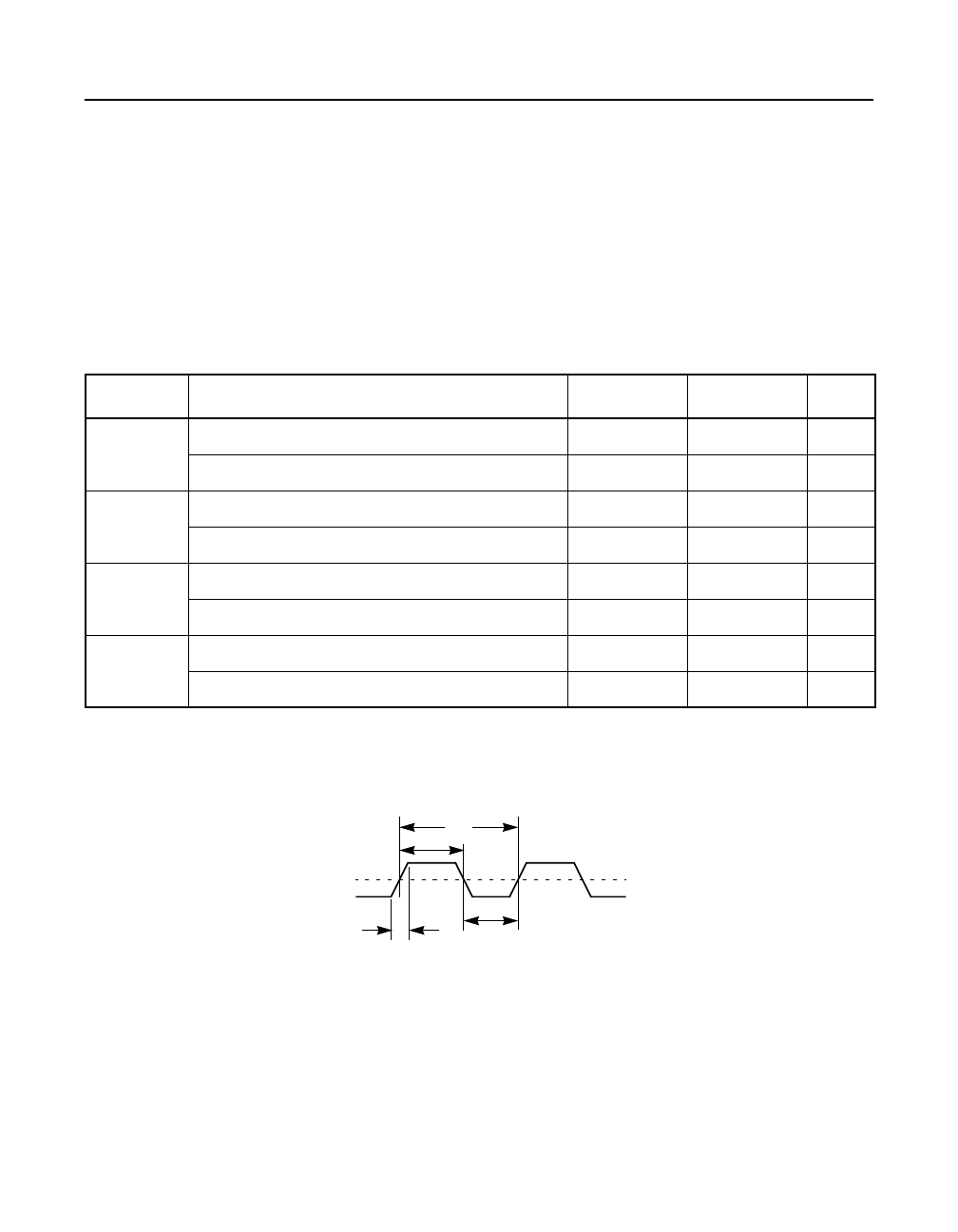
50 pF. Table 7.13 and Figure 7.6 provide clock timing data.
Figure 7.6 Clock Timing
Table 7.13 Clock Timing
Symbol Parameter Min Max Unit
t
1
Bus clock cycle time 30 DC ns
SCSI clock cycle time (SCLK)
1
1. This parameter must be met to ensure SCSI timings are within specification.
25 60 ns
t
2
CLK LOW time
2
2. Duty cycle not to exceed 60/40.
12 – ns
SCLK LOW time
2
10 33 ns
t
3
CLK HIGH time
2
12 – ns
SCLK HIGH time
2
10 33 ns
t
4
CLK slew rate 1 – V/ns
SCLK slew rate 1 – V/ns
CLK, SCLK
t
1
t
3
t
4
t
2