


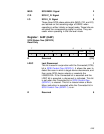
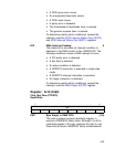
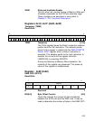
5-33
WRIE Write and Invalidate Enable 0
This bit, when set, causes issuing of Memory Write and
Invalidate commands on the PCI bus whenever legal.
These conditions are described in more detail in
Chapter 3, “PCI Functional Description.”
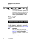
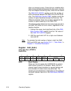
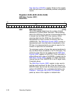
Registers:0x1C–0x1F (0x9C–0x9F)
Temporary (TEMP)
Read/Write
TEMP Temporary [31:0]
This 32-bit register stores the Return instruction address
pointer from the Call instruction. The address pointer
stored in this register is loaded into the DMA SCRIPTS
Pointer (DSP) register when a Return instruction is
executed. This address points to the next instruction to
execute. Do not write to this register while the
LSI53C810A is executing SCRIPTS.
During any Memory-to-Memory Move operation, the
contents of this register are preserved. The power-up
value of this register is indeterminate.
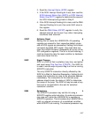
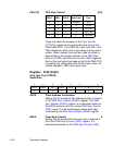
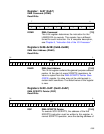
Register: 0x20 (0xA0)
DMA FIFO (DFIFO)
Read/Write
R Reserved 7
BO[6:0] Byte Offset Counter [6:0]
These bits indicate the amount of data transferred
between the SCSI core and the DMA core. It may be
used to determine the number of bytes in the DMA FIFO
31 0
TEMP
xxxxxxxxxxxxxxxxxxxxxxxxxxxxxxxx
7 0
R BO[6:0]
x0000000