PCI Interface Timing Diagrams 7-25
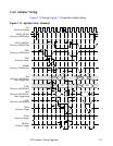
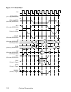
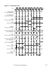
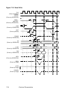
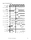
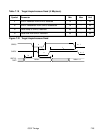
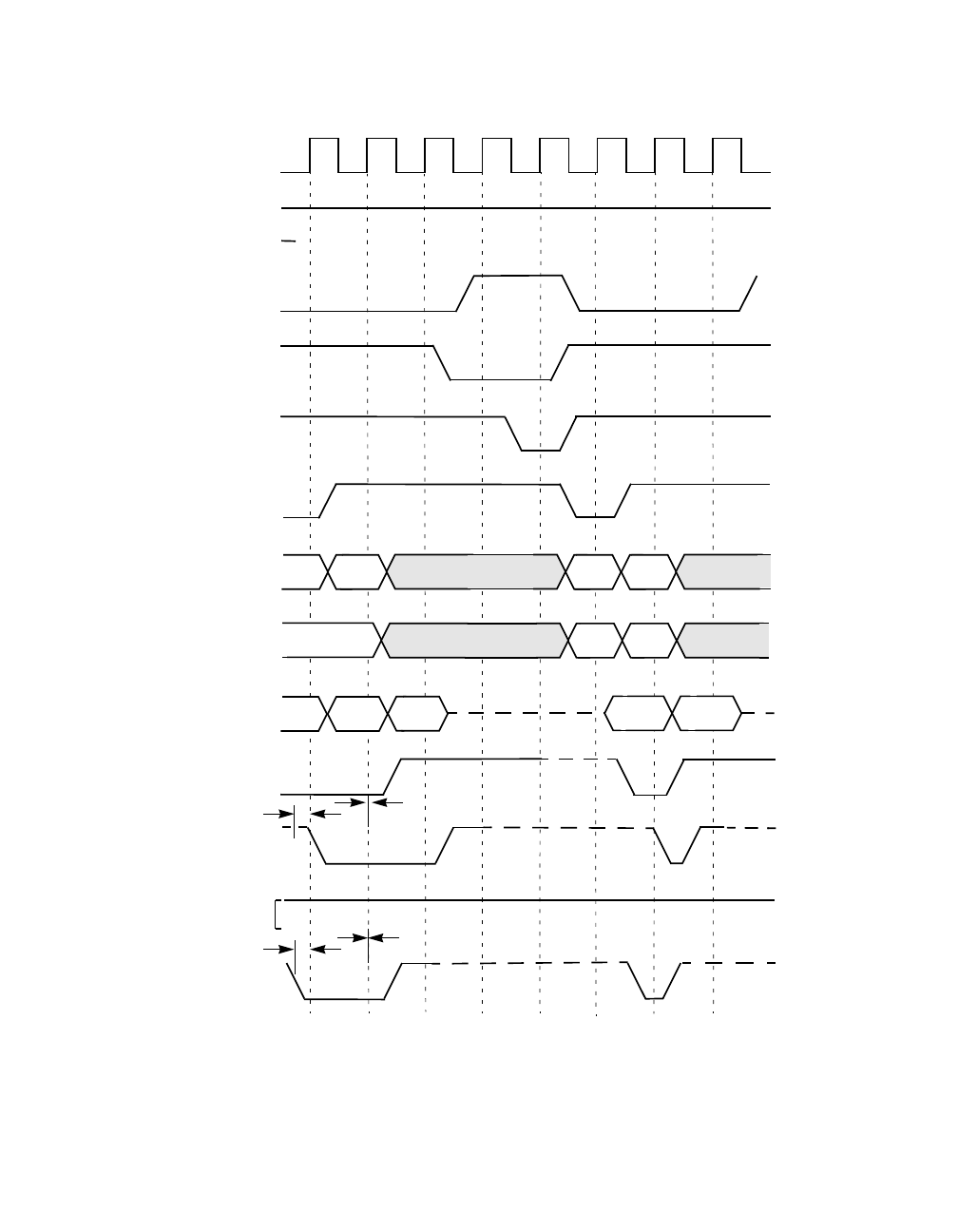
Figure 7.18 Burst Write (Cont.)
t
1
t
2
Addr
Out
BE
Data
Out
CMD
t
1
t
2
BE
Data
Out
Data
Out
CLK
(Driven by System)
GPIO0_
FETCH/
PAR
(Driven by LSI53C810A)
IRDY/
(Driven by LSI53C810A)
TRDY/
(Driven by Target)
STOP/
(Driven by Target)
DEVSEL/
(Driven by Target)
AD
(Driven by LSI53C810A)
C_BE/
(Driven by LSI53C810A)
GNT/
(Driven by Arbiter)
FRAME/
(Driven by LSI53C810A)
(Driven by LSI53C810A)
REQ/
(Driven by LSI53C810A)
GPIO1_
MASTER/
(Driven by LSI53C810A)


