7-12 Electrical Characteristics
7.4 PCI Interface Timing Diagrams
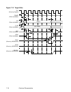
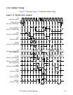
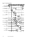
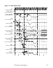
Figure 7.9 through Figure 7.18 represent signal activity when the
LSI53C810A accesses the PCI bus. The timings for the PCI bus interface
are listed on page 7-26. The following timing diagrams are included in
this section:
Target Timing
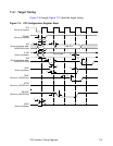
• PCI Configuration Register Read
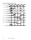
• PCI Configuration Register Write
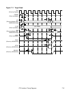
• Target Read
• Target Write
Initiator Timing
• OpCode Fetch, Nonburst
• Burst Opcode Fetch
• Back-to-Back Read
• Back-to-Back Write
• Burst Read
• Burst Write


