


5-36 Operating Registers
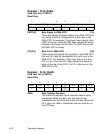
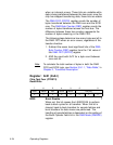
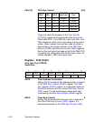
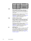
FBL[2:0] FIFO Byte Control [2:0]
These bits steer the contents of the Chip Test Six
(CTEST6) register to the appropriate byte lane of the
32-bit DMA FIFO. If the FBL2 bit is set, then FBL1 and
FBL0 determine which of four byte lanes can be read or
written. When cleared, the byte lane read or written is
determined by the current contents of the DMA Next
Address (DNAD) and DMA Byte Counter (DBC) registers.
Each of the four bytes that make up the 32-bit DMA FIFO
is accessed by writing these bits to the proper value. For
normal operation, FBL2 must equal zero.
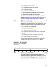
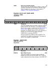
Register: 0x22 (0xA2)
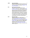
Chip Test Five (CTEST5)
Read/Write
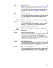
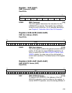
ADCK Clock Address Incrementor 7
Setting this bit increments the address pointer contained
in the DMA Next Address (DNAD) register. The DMA
Next Address (DNAD) register is incremented based on
the DNAD contents and the current DMA Byte Counter
(DBC) value. This bit automatically clears itself after
incrementing the DMA Next Address (DNAD) register.
BBCK Clock Byte Counter 6
Setting this bit decrements the byte count contained in
the 24-bit DMA Byte Counter (DBC) register. It is
decremented based on the DMA Byte Counter (DBC)
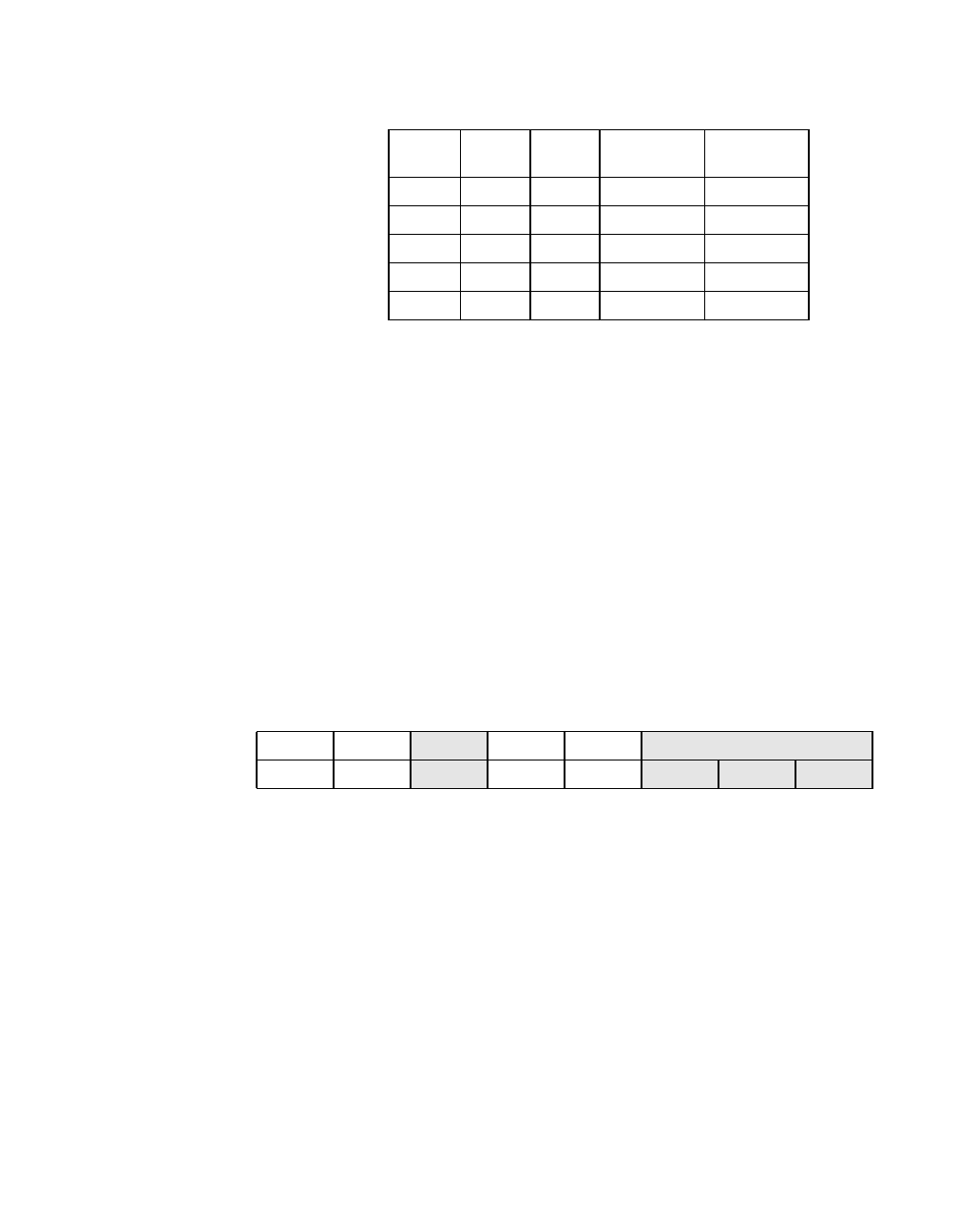
FBL2 FBL1 FBL0
DMA FIFO
Byte Lane Pins
x x x Disabled N/A
0 0 0 0 D[7:0]
0 0 1 1 D[15:8]
0 1 0 2 D[23:16]
0 1 1 3 D[31:24]
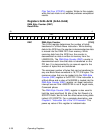
765432 0
ADCK BBCK R MASR DDIR R
00x00x x x