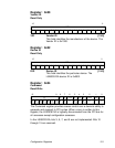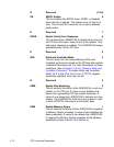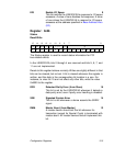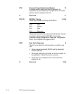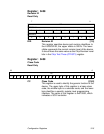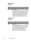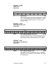
3-10 PCI Functional Description
Note: The configuration register descriptions are provided for
general information only, to indicate which PCI
configuration addresses are supported in the LSI53C810A.
For detailed information, refer to the PCI Specification.
All PCI-compliant devices, such as the LSI53C810A, must support the
Vendor ID, Device ID, Command, and Status registers. Support of other
PCI-compliant registers is optional. In the LSI53C810A, registers that are
not supported are not writable and return all zeros when read. Only those
registers and bits that are currently supported by the LSI53C810A are
described in this chapter.
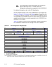
Table 3.2 contains a list of the PCI configuration registers supported in
the LSI53C810A. Addresses 0x40 through 0x7F are not defined.
Table 3.2 PCI Configuration Register Map
31 16 15 0
Device ID Vendor ID 0x00
Status Command 0x04
Class Code Revision ID 0x08
Not Supported Header Type Latency Timer Cache Line Size 0x0C
Base Address Zero (I/O)
1
1. I/O Base is supported.
0x10
Base Address One (Memory)
2
2. Memory Base is supported.
Note: Addresses 0x40 to 0x7F are not defined. All unsupported registers are not writable and return all
zeros when read. Reserved registers also return zeros when read.
0x14
Not Supported 0x18
Not Supported 0x1C
Not Supported 0x20
Not Supported 0x24
Reserved 0x28
Reserved 0x2C
Reserved 0x30
Reserved 0x34
Reserved 0x38
Max_Lat Min_Gnt Interrupt Pin Interrupt Line 0x3C


