3-12 PCI Functional Description
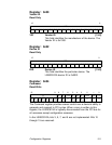
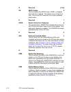
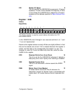
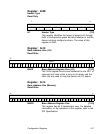
R Reserved [15:9]
SE SERR/ Enable 8
This bit enables the SERR/ driver. SERR/ is disabled
when this bit is cleared. The default value of this bit is
zero. This bit and bit 6 must be set to report address
parity errors.
R Reserved 7
EPER Enable Parity Error Response 6
This bit allows the LSI53C810A to detect parity errors on
the PCI bus and report these errors to the system. Only
data parity checking is enabled. The LSI53C810A always
generates parity for the PCI bus.
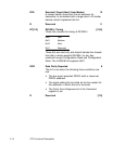
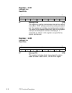
R Reserved 5
WIE Write and Invalidate Mode 4
This bit, when set, will cause Memory Write and
Invalidate cycles to be issued on the PCI bus after certain
conditions have been met. For more information on these
conditions, refer to Section 3.2.3.2, “Memory Write and
Invalidate Command.” To enable Write and Invalidate
Mode, bit 0 in the Chip Test Three (CTEST3) register
(operating registers) must also be set.
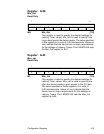
R Reserved 3
EBM Enable Bus Mastering 2
This bit controls the ability of the LSI53C810y to act as a
master on the PCI bus. A value of zero disables the
device from generating PCI bus master accesses. A
value of one allows the LSI53C810A to behave as a bus
master. The LSI53C810A must be a bus master in order
to fetch SCRIPTS instructions and transfer data.
EMS Enable Memory Space 1
This bit controls the ability of the LSI53C810A to respond
to Memory Space accesses. A value of zero disables the
device response. A value of one allows the LSI53C810A
to respond to Memory Space accesses at the address
specified by Base Address One (Memory).


