


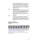
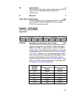
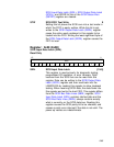
5-61
SOM SCSI Synchronous Offset Maximum 0
This bit indicates that the current synchronous
SREQ/SACK offset is the maximum specified by bits [3:0]
in the SCSI Transfer (SXFER) register. This bit is not
latched and may change at any time. It is used in low
level synchronous SCSI operations. When this bit is set,
the LSI53C810A, as a target, is waiting for the initiator to
acknowledge the data transfers. If the LSI53C810A is an
initiator, then the target has sent the offset number of
requests.
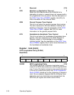
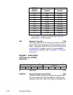
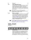
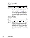
Register: 0x4D (0xCD)
SCSI Test One (STEST1)
Read/Write
SCLK SCSI Clock 7
When set, this bit disables the external SCLK (SCSI
Clock) pin, and the chip uses the PCI clock as the
internal SCSI clock. If a transfer rate of 10 Mbytes/s is
desired on the SCSI bus, this bit must be cleared and the
chip must be connected to at least a 40 MHz external
SCLK.
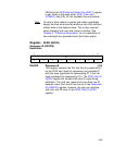
SISO SCSI Isolation Mode 6
This bit allows the LSI53C810A to put the SCSI
bidirectional and input pins into a low power mode when
the SCSI bus is not in use. When this bit is set, the SCSI
bus inputs are logically isolated from the SCSI bus.
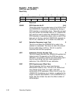
R Reserved [5:0]
765 0
SCLK SISO R
00x x x x x x