


4-6 Signal Descriptions
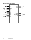
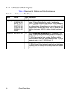
4.1.2 Address and Data Signals
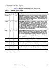
Table 4.3 describes the Address and Data Signals group.
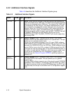
Table 4.3 Address and Data Signals
Name Pin No. Type Description
AD[31:0] 85, 86, 88, 89,
91, 92, 94, 95,
98, 100, 1, 2, 4,
6, 7, 8, 23, 24,
25, 27, 29, 30,
31, 33, 35, 36,
38, 39, 41, 42,
44, 45
T/S Physical Dword Address and Data are multiplexed on the
same PCI pins. During the first clock of a transaction,
AD[31:0] contain a physical byte address. During subsequent
clocks, AD[31:0] contain data. A bus transaction consists of
an address phase followed by one or more data phases. PCI
supports both read and write bursts. AD[7:0] define the least
significant byte, and AD[31:24] define the most significant
byte.
C_BE/[3:0] 96, 10, 21, 34 T/S Bus Command and Byte Enables are multiplexed on the
same PCI pins. During the address phase of a transaction,
C_BE/[3:0] define the bus command. During the data phase,
C_BE/[3:0] are used as byte enables. The byte enables
determine which byte lanes carry meaningful data. C_BE/[0]
applies to byte 0, and C_BE/[3] to byte 3.
PAR 20 T/S Parity is the even parity bit that protects the AD[31:0] and
C_BE/[3:0] lines. During address phase, both the address and
command bits are covered. During data phase, both data and
byte enables are covered.