4-10 Signal Descriptions
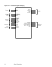
4.2.2 Additional Interface Signals
Table 4.8 describes the Additional Interface Signals group.
Table 4.8 Additional Interface Signals
Name Pin No. Type Description
TESTIN/ 52 I Test In. When this pin is driven LOW, the LSI53C810A connects all
inputs and outputs to an “AND tree.” The SCSI control signals and data
lines are not connected to the “AND tree.” The output of the “AND tree”
is connected to the Test Out pin. This allows manufacturers to verify
chip connectivity and determine exactly which pins are not properly
attached. When the TESTIN pin is driven LOW, internal pull-ups are
enabled on all input, output, and bidirectional pins, all outputs and
bidirectional signals will be 3-stated, and the MAC/_TESTOUT pin will
be enabled. Connectivity can be tested by driving one of the
LSI53C810A pins LOW. The MAC/_TESTOUT pin should respond by
also driving LOW.
GPIO0_
FETCH/
48 I/O General Purpose I/O pin. Optionally, when driven LOW, this pin
indicates that the next bus request will be for an opcode fetch. This pin
powers up as a general purpose input.
This pin has two specific purposes in the LSI Logic SDMS software.
SDMS software uses it to toggle SCSI device LEDs, turning on the LED
whenever the LSI53C810A is on the SCSI bus. SDMS software drives
this pin LOW to turn on the LED, or drives it HIGH to turn off the LED.
This signal can also be used as data I/O for serial EEPROM access. In
this case it is used with the GPIO0 pin, which serves as a clock, and
the pin can be controlled from PCI configuration register 0x35 or
observed from the General Purpose (GPREG) operating register, at
address 0x07.
GPIO1_
MASTER/
49 I/O General Purpose I/O pin. Optionally, when driven LOW, indicates that
the LSI53C810A is bus master. This pin powers up as a general
purpose input.
LSI Logic SDMS software supports use of this signal in serial EEPROM
applications, when enabled, in combination with the GPIO0 pin. When
this signal is used as a clock for serial EEPROM access, the GPIO1 pin
serves as data, and the pin is controlled from PCI configuration register
0x35.


