


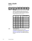
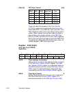
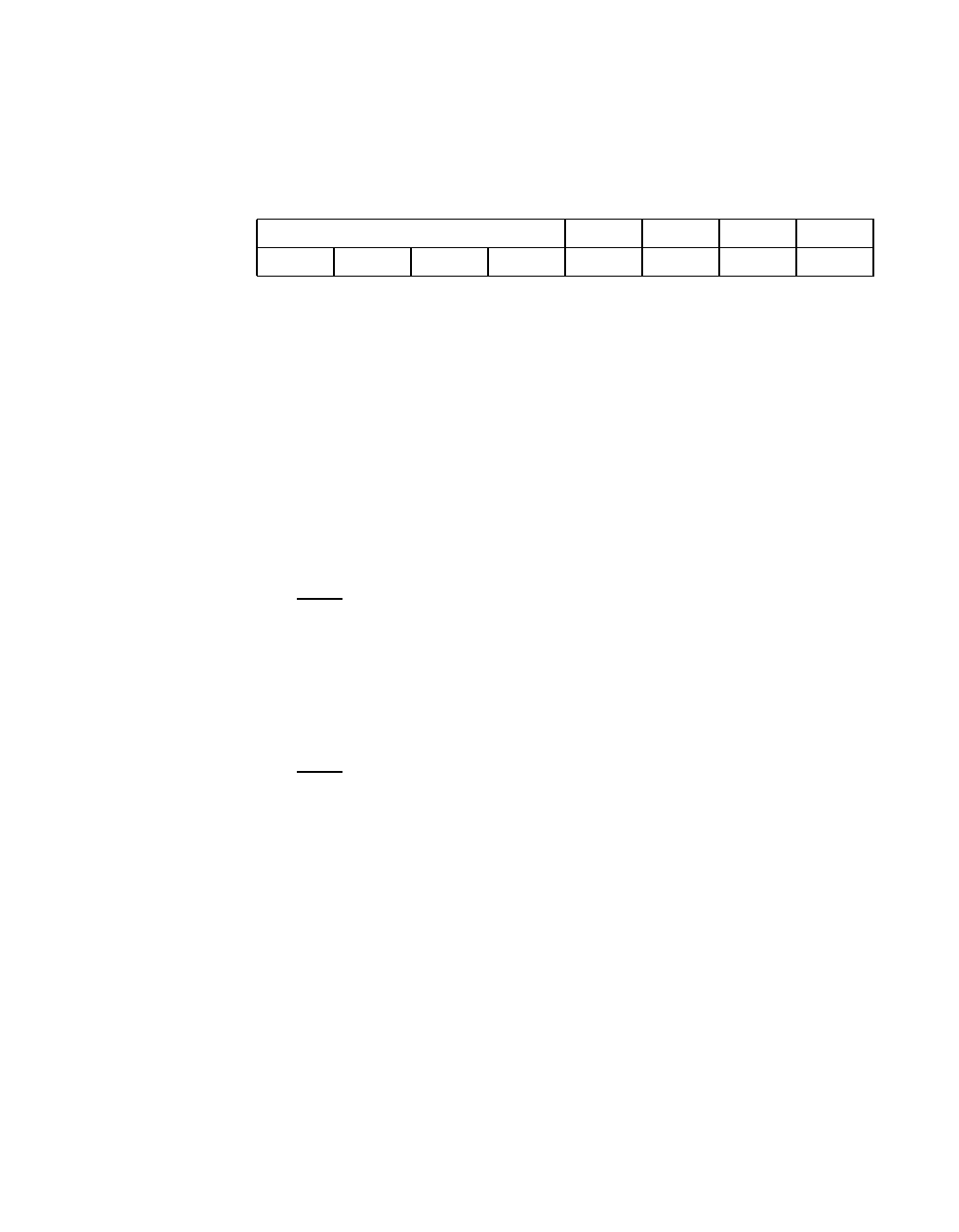
5-32 Operating Registers
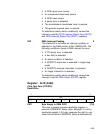
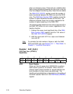
Register: 0x1B (0x9B)
Chip Test Three (CTEST3)
Read/Write
V[3:0] Chip Revision Level [7:4]
These bits identify the chip revision level for software
purposes.
FLF Flush DMA FIFO 3
When this bit is set, data residing in the DMA FIFO is
transferred to memory, starting at the address in the DMA
Next Address (DNAD) register. The internal DMAWR
signal, controlled by the Chip Test Five (CTEST5)
register, determines the direction of the transfer. This bit
is not self-clearing; clear it once the data is successfully
transferred by the LSI53C810A.
Note: Polling of FIFO flags is allowed during flush operations.
CLF Clear DMA FIFO 2
When this bit is set, all data pointers for the DMA FIFO
are cleared. Any data in the FIFO is lost. After the
LSI53C810A successfully clears the appropriate FIFO
points and registers, this bit automatically clears.
Note: This bit does not clear the data visible at the bottom of the
FIFO.
FM Fetch Pin Mode 1
When set, this bit causes the FETCH/ pin to deassert
during indirect and table indirect read operations.
FETCH/ is only active during the opcode portion of an
instruction fetch. This allows the storage of SCRIPTS in
a PROM while data tables are stored in RAM.
If this bit is not set, FETCH/ is asserted for all bus cycles
during instruction fetches.
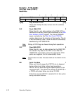
7 43210
V[3:0] FLF CLF FM WRIE
xxxx0000