PCI Cache Mode 3-7
If cache mode is enabled, a Read Line command is issued on all read
cycles, except opcode fetches, when the following conditions are met:
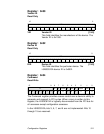
• The CLSE (Cache Line Size Enable, bit 7, DMA Control (DCNTL)
register) and ERL (Enable Read Line, bit 3, DMA Mode (DMODE)
register) bits are set.
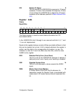
• The Cache Line Size register must contain a legal burst size value
(2, 4, 8 or 16) and that value is less than or equal to the DMA Mode
(DMODE) burst size.
• The number of bytes to be transferred at the time a cache boundary
is reached must be equal to or greater than a full cache line size.
• The chip is aligned to a cache line boundary.
When these conditions are met, the chip issues a Read Line command
instead of a Memory Read during all PCI read cycles. Otherwise, it
issues a normal Memory Read command.
3.2.4 Memory Read Multiple Command
This command is identical to the Memory Read command except that it
additionally indicates that the master may intend to fetch more than one
cache line before disconnecting. The LSI53C810A supports PCI Read
Multiple functionality and issues Read Multiple commands on the PCI
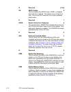
bus when the Read Multiple Mode is enabled. This mode is enabled by
setting bit 2 (ERMP) of the DMA Mode (DMODE) register. The command
is issued when certain conditions are met.
If cache mode is enabled, a Read Multiple command is issued on all read
cycles, except opcode fetches, when the following conditions are met:
1. The CLSE bit (Cache Line Size Enable, bit 7, DMA Control (DCNTL)
register) and the ERMP bit (Enable Read Multiple, bit 2, DMA Mode
(DMODE) register) are set.
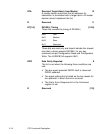
2. The Cache Line Size register contains a legal burst size value (2, 4,
8 or 16) and that value is less than or equal to the DMA Mode
(DMODE) burst size.
3. The number of bytes to be transferred at the time a cache boundary
is reached is equal to or greater than the DMA Mode (DMODE) burst
size.
4. The chip is aligned to a cache line boundary.


