


5-37
contents and the current DNAD value. This bit
automatically clears itself after decrementing the DMA
Byte Counter (DBC) register.
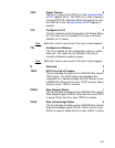
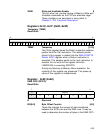
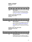
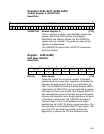
R Reserved 5
MASR Master Control for Set or Reset Pulses 4
This bit controls the operation of bit 3. When this bit is
set, bit 3 asserts the corresponding signals. When this bit
is cleared, bit 3 deasserts the corresponding signals. Do
not change this bit and bit 3 in the same write cycle.
DDIR DMA Direction 3
Setting this bit either asserts or deasserts the internal
DMA Write (DMAWR) direction signal depending on the
current status of the MASR bit in this register. Asserting
the DMAWR signal indicates that data is transferred from
the SCSI bus to the host bus. Deasserting the DMAWR
signal transfers data from the host bus to the SCSI bus.
R Reserved [2:0]
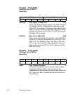
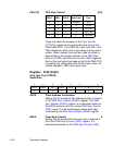
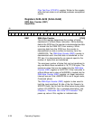
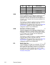
Register: 0x23 (0xA3)
Chip Test Six (CTEST6)
Read/Write
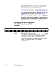
DF DMA FIFO [7:0]
Writing to this register writes data to the appropriate byte
lane of the DMA FIFO as determined by the FBL bits in
the Chip Test Four (CTEST4) register. Reading this
register unloads data from the appropriate byte lane of
the DMA FIFO as determined by the FBL bits in the Chip
Test Four (CTEST4) register. Data written to the FIFO is
loaded into the top of the FIFO. Data read out of the FIFO
is taken from the bottom. To prevent DMA data from
being corrupted, this register should not be accessed
before starting or restarting SCRIPTS operation. Write
this register only when testing the DMA FIFO using the
7 0
DF
00000000