5-42 Operating Registers
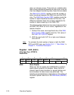
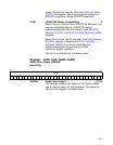
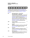
SIOM Source I/O Memory Enable 5
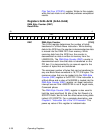
This bit is defined as an I/O Memory Enable bit for the
source address of a Memory Move or Block Move
Command. If this bit is set, then the source address is in
I/O space; and if cleared, then the source address is in
memory space.
This function is useful for register-to-memory operations
using the Memory Move instruction when the
LSI53C810A is I/O mapped. Bits 4 and 5 of the Chip Test
Two (CTEST2) register are used to determine the
configuration status of the LSI53C810A.
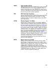
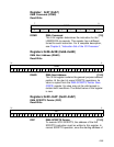
DIOM Destination I/O Memory Enable 4
This bit is defined as an I/O Memory Enable bit for the
destination address of a Memory Move or Block Move
Command. If this bit is set, then the destination address
is in I/O space; and if cleared, then the destination
address is in memory space.
This function is useful for memory-to-register operations
using the Memory Move instruction when the
LSI53C810A is I/O mapped. Bits 4 and 5 of the Chip Test
Two (CTEST2) register are used to determine the
configuration status of the LSI53C810A.
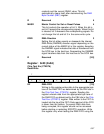
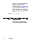
ERL Enable Read Line 3
This bit enables a PCI Read Line command. If PCI cache
mode is enabled by setting bits in the PCI Cache Line
Size register, the chip issues a Read Line command on
all read cycles if other conditions are met. For more
information on these conditions, refer to Chapter 3, “PCI
Functional Description.”
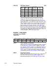
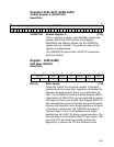
BL1 BL0 Burst Length
0 0 2-transfer burst
0 1 4-transfer burst
1 0 8-transfer burst
1 1 16-transfer burst


