3-4 PCI Functional Description
3.2.2 Selection of Cache Line Size
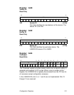
The cache logic selects a cache line size based on the values for the
burst size in the DMA Mode (DMODE) register and the PCI Cache Line
Size register.
Note: The LSI53C810A does not automatically use the value in
the PCI Cache Line Size register as the cache line size
value. The chip scales the value of the Cache Line Size
register down to the nearest binary burst size allowed by
the chip (2, 4, 8 or 16), compares this value to the DMODE
burst size, then selects the smallest as the value for the
cache line size. The LSI53C810A uses this value for all
burst data transfers.
3.2.3 Alignment
The LSI53C810A uses the calculated burst size value to monitor the
current address for alignment to the cache line size. When it is not
aligned, the chip disables bursting allowing only single Dword transfers
until a cache line boundary is reached. When the chip is aligned, bursting
is re-enabled allowing bursts in increments specified by the Cache Line
Size register as explained above. If the Cache Line Size register is not
set (default = 0x00), the DMODE burst size is automatically used as the
cache line size.
3.2.3.1 MMOV Misalignment
The LSI53C810A does not operate in a cache alignment mode when a
MMOV instruction is issued and the read and write addresses are
different distances from the nearest cache line boundary. For example, if
the read address is 0x21F and the write address is 0x42F, and the cache
line size is eight (8), the addresses are byte aligned, but they are not the
same distance from the nearest cache boundary. The read address is 1
byte from the cache boundary 0x220 and the write address is 17 bytes
from the cache boundary 0x440. In this situation, the chip does not align
to cache boundaries and operates as an LSI53C810.


