


5-41
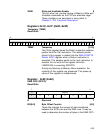
Registers:0x34–0x37 (0xB4–0xB7)
Scratch Register A (SCRATCHA)
Read/Write
SCRATCHA Scratch Register A [31:0]
This is a general purpose, user-definable scratch pad
register. Apart from CPU access, only Register
Read/Write and Memory Moves into the SCRATCH
register alter its contents. The power-up value of this
register is indeterminate.
The LSI53C810A cannot fetch SCRIPTS instructions
from this location.
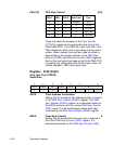
Register: 0x38 (0xB8)
DMA Mode (DMODE)
Read/Write
BL[1:0] Burst Length [7:6]
These bits control the maximum number of transfers
performed per bus ownership, regardless of whether the
transfers are back-to-back, burst, or a combination of
both. The LSI53C810A asserts the Bus Request (REQ/)
output when the DMA FIFO can accommodate a transfer
of at least one burst size of data. Bus Request (REQ/) is
also asserted during start-of-transfer and end-of-transfer
cleanup and alignment, even though less than a full burst
of transfers is performed. The LSI53C810A inserts a
“fairness delay” of four CLKs between burst-length
transfers (as set in BL[1:0]) during normal operation. The
fairness delay is not inserted during PCI retry cycles. This
gives the CPU and other bus master devices the
opportunity to access the PCI bus between bursts.
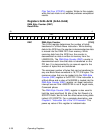
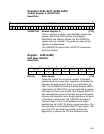
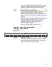
31 0
SCRATCHA
xxxxxxxxxxxxxxxxxxxxxxxxxxxxxxxx
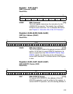
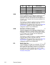
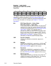
76543210
BL[1:0] SIOM DIOM ER ERMP BOF MAN
00000000