


5-38 Operating Registers
Chip Test Four (CTEST4) register. Writes to this register
while the test mode is not enabled produces unexpected
results.
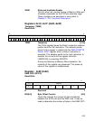
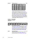
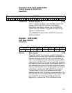
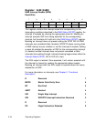
Registers:0x24–0x26 (0xA4–0xA6)
DMA Byte Counter (DBC)
Read/Write
DBC DMA Byte Counter [23:0]
This 24-bit register determines the number of bytes
transferred in a Block Move instruction. While sending
data to the SCSI bus, the counter is decremented as data
is moved into the DMA FIFO from memory. While
receiving data from the SCSI bus, the counter is
decremented as data is written to memory from the
LSI53C810A. The DMA Byte Counter (DBC) counter is
decremented each time that data is transferred on the
PCI bus. It is decremented by an amount equal to the
number of bytes that are transferred.
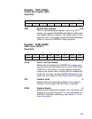
The maximum number of bytes that can be transferred in
any one Block Move command is 16,777,215 bytes. The
maximum value that can be loaded into the DMA Byte
Counter (DBC) register is 0xFFFFFF. If the instruction is
a Block Move and a value of 0x000000 is loaded into the
DMA Byte Counter (DBC) register, an illegal instruction
interrupt occurs if the LSI53C810A is not in target mode,
Command phase.
The DMA Byte Counter (DBC) register is also used to
hold the least significant 24 bits of the first Dword of a
SCRIPTS fetch, and to hold the offset value during table
indirect I/O SCRIPTS. For a complete description, see
Chapter 6, “Instruction Set of the I/O Processor.” The
power-up value of this register is indeterminate.
23 0
DBC
xxxxxxxxxxxxxxxxxxxxxxxx