


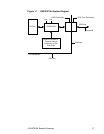
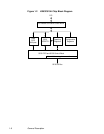

2-4 Functional Description
the prefetch unit contents, use the No Flush Memory to Memory
Move (NFMMOV) instruction for all MMOV operations that do not
modify code within the next 4 to 8 Dwords. For more information on
this instruction, refer to Chapter 6, “Instruction Set of the I/O
Processor.”
• On every Store instruction. The Store instruction may also be used
to place modified code directly into memory. To avoid inadvertently
flushing the prefetch unit contents use the No Flush option for all
Store operations that do not modify code within the next 8 Dwords.
• On every write to the DMA SCRIPTS Pointer (DSP) register.
• On all Transfer Control instructions when the transfer conditions are
met. This is necessary because the next instruction to execute is not
the sequential next instruction in the prefetch unit.
• When the Prefetch Flush bit (DMA Control (DCNTL) bit 6) is set. The
unit flushes whenever this bit is set. The bit is self-clearing.
2.3.1 Opcode Fetch Burst Capability
Setting the Burst Opcode Fetch Enable bit (bit 1) in the DMA Mode
(DMODE) register (0x38) causes the LSI53C810A to burst in the first two
Dwords of all instruction fetches. If the instruction is a Memory-to-
Memory Move, the third Dword is accessed in a separate ownership. If
the instruction is an indirect type, the additional Dword is accessed in a
subsequent bus ownership. If the instruction is a Table Indirect Block
Move, the chip uses two accesses to obtain the four Dwords required, in
two bursts of two Dwords each.
Note: This feature can only be used if SCRIPTS prefetching is
disabled.
2.4 PCI Cache Mode
The LSI53C810A supports the PCI specification for an 8-bit Cache Line
Size register located in PCI configuration space. The Cache Line Size
register provides the ability to sense and react to nonaligned addresses
corresponding to cache line boundaries. In conjunction with the Cache
Line Size register, the PCI commands Read Line, Read Multiple, and