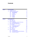
viii Contents
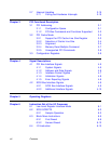
2.7 Interrupt Handling 2-15
2.7.1 Polling and Hardware Interrupts 2-15
Chapter 3 PCI Functional Description
3.1 PCI Addressing 3-1
3.1.1 Configuration Space 3-1
3.1.2 PCI Bus Commands and Functions Supported 3-2
3.2 PCI Cache Mode 3-3
3.2.1 Support for PCI Cache Line Size Register 3-3
3.2.2 Selection of Cache Line Size 3-4
3.2.3 Alignment 3-4
3.2.4 Memory Read Multiple Command 3-7
3.2.5 Unsupported PCI Commands 3-8
3.3 Configuration Registers 3-9
Chapter 4 Signal Descriptions
4.1 PCI Bus Interface Signals 4-5
4.1.1 System Signals 4-5
4.1.2 Address and Data Signals 4-6
4.1.3 Interface Control Signals 4-7
4.1.4 Arbitration Signals 4-8
4.1.5 Error Reporting Signals 4-8
4.2 SCSI Bus Interface Signals 4-9
4.2.1 SCSI Bus Interface Signals 4-9
4.2.2 Additional Interface Signals 4-10
Chapter 5 Operating Registers
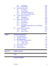
Chapter 6 Instruction Set of the I/O Processor
6.1 Low Level Register Interface Mode 6-1
6.2 SCSI SCRIPTS 6-2
6.2.1 Sample Operation 6-3
6.3 Block Move Instructions 6-5
6.3.1 First Dword 6-6
6.3.2 Second Dword 6-12
6.4 I/O Instruction 6-13


