1-6 General Description
• Controlled bus assertion times (reduces RFI, improves reliability, and
eases FCC certification)
• Latch-up protection greater than 150 mA
• Voltage feed-through protection (minimum leakage current through
SCSI pads)
• High proportion (> 25%) of pins power and ground
• Power and ground isolation of I/O pads and internal chip logic
• TolerANT technology, which provides:
– Active negation of SCSI Data, Parity, Request, and Acknowledge
signals for improved fast SCSI transfer rates.
– Input signal filtering on SCSI receivers improves data integrity,
even in noisy cabling environments.
1.2.7 Testability
The LSI53C810A provides improved testability through:
• Access to all SCSI signals through programmed I/O
• SCSI loopback diagnostics
• SCSI bus signal continuity checking
• Support for single step mode operation
• Test mode (AND tree) to check pin continuity to the board
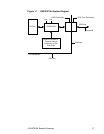
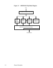
A system diagram showing the connections of the LSI53C810A in a PCI
system is pictured in Figure 1.1. A block diagram of the LSI53C810A is
pictured in Figure 1.2.


