Parity Options 2-5
Write and Invalidate are each software enabled or disabled to allow the
user full flexibility in using these commands. For more information on PCI
cache mode operations, refer to Chapter 3, “PCI Functional Description.”
2.4.1 Load and Store Instructions
The LSI53C810A supports the Load and Store instruction type, which
simplifies the movement of data between memory and the internal chip
registers. It also enables the LSI53C810A to transfer bytes to addresses
relative to the Data Structure Address (DSA) register. For more
information on the Load and Store instructions, refer to
Chapter 6, “Instruction Set of the I/O Processor.”
2.4.2 3.3 V/5 V PCI Interface
The LSI53C810A can attach directly to a 3.3 V or a 5 V PCI interface,
due to separate V
DD
pins for the PCI bus drivers. This allows the devices
to be used on the universal board recommended by the PCI Special
Interest Group.
2.4.3 Loopback Mode
The LSI53C810A loopback mode allows testing of both initiator and
target functions and, in effect, lets the chip communicate with itself.
When the Loopback Enable bit is set in the SCSI Test Two (STEST2)
register, bit 4, the LSI53C810A allows control of all SCSI signals whether
the chip is operating in the initiator or target mode. For more information
on this mode of operation refer to the
SCSI SCRIPTS Processors
Programming Guide
.
2.5 Parity Options
The LSI53C810A implements a flexible parity scheme that allows control
of the parity sense, allows parity checking to be turned on or off, and has
the ability to deliberately send a byte with bad parity over the SCSI bus
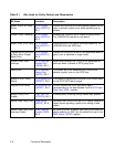
to test parity error recovery procedures. Table 2.1 defines the bits that
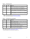
are involved in parity control and observation. Table 2.2 describes the
parity control function of the Enable Parity Checking and Assert SCSI
Even Parity bits in the SCSI Control Zero (SCNTL0) register. Table 2.3
describes the options available when a parity error occurs.


