


5-34 Operating Registers
when an interrupt occurs. These bits are unstable while
data is being transferred between the two cores; once the
chip has stopped transferring data, these bits are stable.
The DMA FIFO (DFIFO) register counts the number of
bytes transferred between the DMA core and the SCSI
core. The DMA Byte Counter (DBC) register counts the
number of bytes transferred across the host bus. The
difference between these two counters represents the
number of bytes remaining in the DMA FIFO.
The following steps determine how many bytes are left in
the DMA FIFO when an error occurs, regardless of the
transfer direction:
1. Subtract the seven least significant bits of the DMA
Byte Counter (DBC) register from the 7-bit value of
the DMA FIFO (DFIFO) register.
2. AND the result with 0x7F for a byte count between
zero and 64.
Note: To calculate the total number of bytes in both the DMA
FIFO and SCSI logic, see Section 2.5.1.1, “Data Paths,” in
Chapter 2, “Functional Description.”
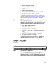
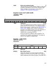
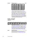
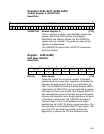
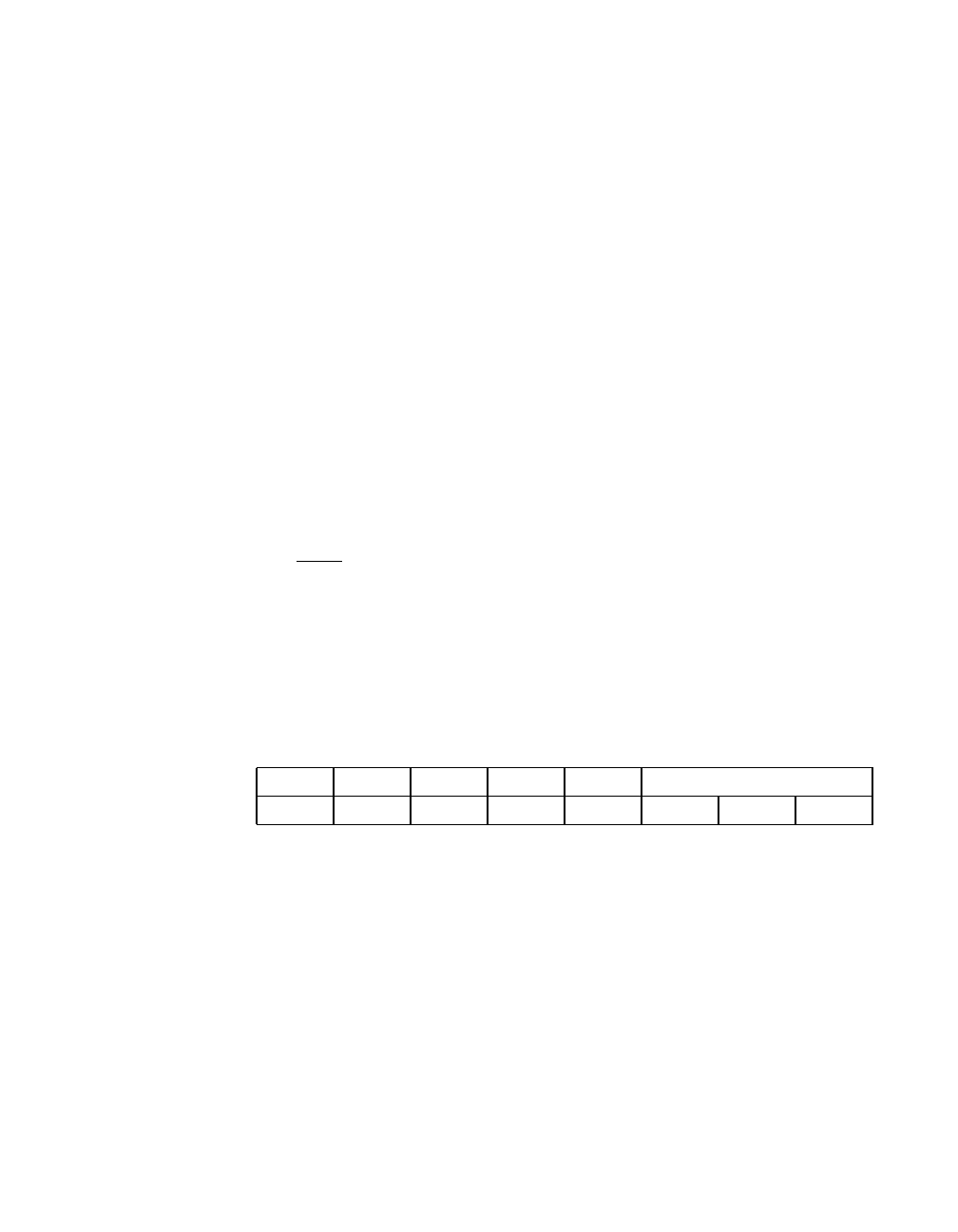
Register: 0x21 (0xA1)
Chip Test Four (CTEST4)
Read/Write
BDIS Burst Disable 7
When set, this bit causes the LSI53C810A to perform
back-to-back cycles for all transfers. When this bit is
cleared, back-to-back transfers for opcode fetches and
burst transfers for data moves are performed. The
handling of opcode fetches is dependent on the setting of
the Burst Opcode Fetch bit in the DMA Mode (DMODE)
register.
765432 0
BDIS ZMOD ZSD SRTM MPEE FBL[2:0]
00000000