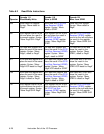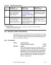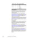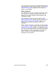
6-30 Instruction Set of the I/O Processor
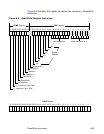
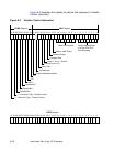
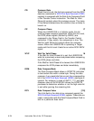
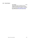
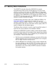
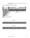
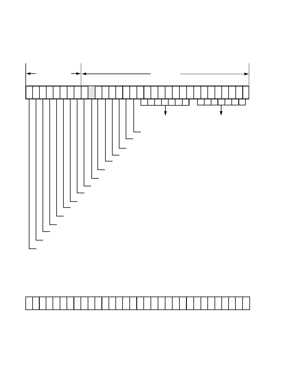
Figure 6.5 illustrates the register bit values that represent a Transfer
Control instruction.
Figure 6.5 Transfer Control Instruction
31 30
29 28 27 26 25 24 23 22 21 20 19 18 17 16 15 14 13 12 11 10 9 8 7 6 5 4 3 2 1
0
31 30
29 28 27 26 25 24 23 22 21 20 19 18 17 16 15 14 13 12 11 10 9 8 7 6 5 4 3 2 1
0
DSPS Register
DCMD Register DBC Register
Wait for Valid Phase
Compare Phase
Compare Data
Jump if: True=1, False=0
Interrupt on the Fly
Carry Test
0 (Reserved)
Relative Addressing Mode
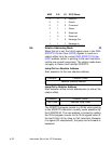
I/O
C/D
MSG
Opcode Bit 0
Opcode Bit 1
Opcode Bit 2
1 - Instruction Type - Transfer Control
0 - Instruction Type - Transfer Control
Mask for Compare
Data to be compared
with the SCSI First
Byte Received


