SCSI Bus Interface 2-13
2.6.3 Synchronous Operation
The LSI53C810A can transfer synchronous SCSI data in both the
initiator and target modes. The SCSI Transfer (SXFER) register controls
both the synchronous offset and the transfer period. It may be loaded by
the CPU before SCRIPTS execution begins, from within SCRIPTS using
a Table Indirect I/O instruction, or with a Read-Modify-Write instruction.
The LSI53C810A can receive data from the SCSI bus at a synchronous
transfer period as short as 80 ns or 160 ns (with a 50 MHz clock),
regardless of the transfer period used to send data. The LSI53C810A
can receive data at one-fourth of the divided SCLK frequency. Depending
on the SCLK frequency, the negotiated transfer period, and the
synchronous clock divider, the LSI53C810A can send synchronous data
at intervals as short as 100 ns for fast SCSI-2 and 200 ns for SCSI-1.
2.6.3.1 Determining the Data Transfer Rate
Synchronous data transfer rates are controlled by bits in two different
registers of the LSI53C810A. Following is a brief description of the bits.
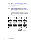
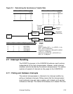
Figure 2.4 illustrates the clock division factors used in each register, and
the role of the register bits in determining the transfer rate.
2.6.3.2 SCNTL3 Register, Bits [6:4] (SCF[2:0])
The SCF[2:0] bits select the factor by which the frequency of SCLK is
divided before being presented to the synchronous SCSI control logic.
The output from this divider controls the rate at which data can be
received; this rate must not exceed 50 MHz. The receive rate is
one-fourth of the divider output. For example, if SCLK is 40 MHz and the
SCF value is set to divide by one, then the maximum rate at which data
can be received is 10 Mbytes/s (40/(1*4) = 10).
For synchronous send, the output of the SCF divider is divided by the
transfer period (XFERP) bits in the SCSI Transfer (SXFER) register. For
valid combinations of the SCF and the XFERP, see Table 5.3 and
Table 5.4, under the description of the XFERP bits [7:5] in the SCSI
Transfer (SXFER) register.


