


BUS INTERFACE UNIT
3-20
An idle bus state may or may not drive the bus. An idle bus state following a bus read cycle con-
tinues to float the bus. An idle bus state following a bus write cycle continues to drive the bus.
The BIU drives no control strobes active in an idle state except to indicate the start of another bus
cycle.
3.5 BUS CYCLES
There are four basic types of bus cycles: read, write, interrupt acknowledge and halt. Interrupt
acknowledge and halt bus cycles define special bus operations and require separate discussions.
Read bus cycles include memory, I/O and instruction prefetch bus operations. Write bus cycles
include memory and I/O bus operations. All read and write bus cycles have the same basic format.
The following sections present timing equations containing symbols found in the data sheet. The
timing equations provide information necessary to start a worst-case design analysis.
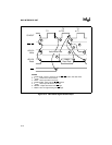
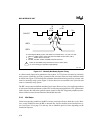
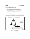
3.5.1 Read Bus Cycles
Figure 3-19 illustrates a typical read cycle. Table 3-2 lists the three types of read bus cycles.
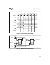
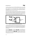
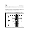
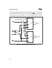
Figure 3-20 illustrates a typical 16-bit interface connection to a read-only device interface. The
same example applies to an 8-bit bus system, except that no devices connect to an upper bus. Four
parameters (Table 3-3) must be evaluated when determining the compatibility of a memory (or
I/O) device. T
ADLTCH
defines the delay through the address latch.
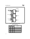
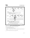
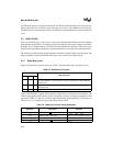
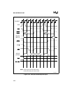
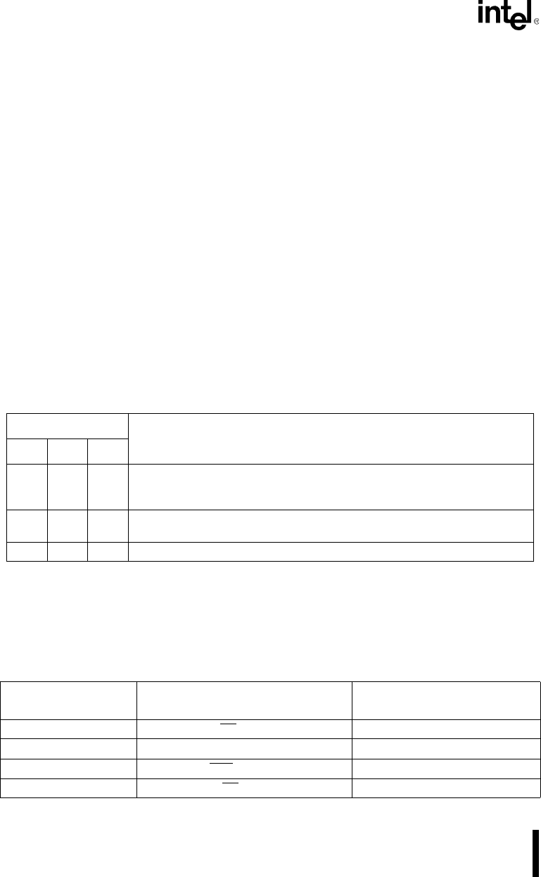
Table 3-2. Read Bus Cycle Types
Status Bit
Bus Cycle Type
S2 S1 S0
0 0 1 Read I/O — Initiated by the Execution Unit for IN, OUT, INS, OUTS instructions
or by the DMA Unit. A19:16 are driven to zero (see Chapter 10, “Direct Memory
Access Unit”).
1 0 0 Instruction Prefetch — Initiated by the BIU. Data read from the bus fills the
prefetch queue.
1 0 1 Read Memory — A19:0 select the desired byte or word memory location.
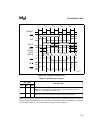
Table 3-3. Read Cycle Critical Timing Parameters
Memory Device
Parameter
Description Equation
T
OE
Output enable (RD low) to data valid 2T
CLCL
– T
CLRL
– T
DVCL
T
ACC
Address valid to data valid 3T
CLCL
– T
CLAV
–T
ADLTCH –
T
DVCL
T
CE
Chip enable (UCS) to data valid 3T
CLCL
– T
CLOV2
– T
CLIS
T
DF
Output disable (RD high) to output float T
RHAV