


7-5
REFRESH CONTROL UNIT
7.5 REFRESH BUS CYCLES
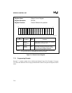
Refresh bus cycles look exactly like ordinary memory read bus cycles except for the control sig-
nals listed in Table 7-1. These signals can be ANDed in a DRAM controller to detect a refresh
bus cycle. The 16-bit bus processor drives both the BHE
and A0 pins high during refresh cycles.
The 8-bit bus version replaces the BHE
pin with RFSH, which has the same timings. The 8-bit
bus processor drives RFSH
low and A0 high during refresh cycles.
7.6 GUIDELINES FOR DESIGNING DRAM CONTROLLERS
The basic DRAM access method consists of four phases:
1. The DRAM controller supplies a row address to the DRAMs.
2. The DRAM controller asserts a Row Address Strobe (RAS
), which latches the row
address inside the DRAMs.
3. The DRAM controller supplies a column address to the DRAMs.
4. The DRAM controller asserts a Column Address Strobe (CAS
), which latches the column
address inside the DRAMs.
Most 80C186 Modular Core family DRAM interfaces use only this method. Others are not dis-
cussed here.
The DRAM controller’s purpose is to use the processor’s address, status and control lines to gen-
erate the multiplexed addresses and strobes. These signals must be appropriate for three bus cycle
types: read, write and refresh. They must also meet specific pulse width, setup and hold timing
requirements. DRAM interface designs need special attention to transmission line effects, since
DRAMs represent significant loads on the bus.
DRAM controllers may be either clocked or unclocked. An unclocked DRAM controller requires
a tapped digital delay line to derive the proper timings.
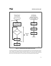
Clocked DRAM controllers may use either discrete or programmable logic devices. A state ma-
chine design is appropriate, especially if the circuit must provide wait state control (beyond that
possible with the processor’s Chip-Select Unit). Because of the microprocessor’s four-clock bus,
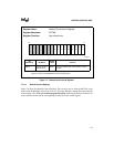
clocking some logic elements on each CLKOUT phase is advantageous (see Figure 7-4).
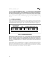
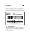
Table 7-1. Identification of Refresh Bus Cycles
Data Bus Width BHE/RFSH A0
16-Bit Device 1 1
8-Bit Device 0 1