


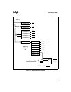
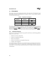
CHIP-SELECT UNIT
6-4
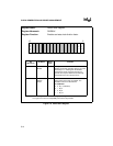
UCS Mapped only to the upper memory address space; selects the BOOT memory
device (EPROM or Flash memory types).
LCS
Mapped only to the lower memory address space; selects a static memory
(SRAM) device that stores the interrupt vector table, local stack, local data, and
scratch pad data.
MCS3:0
Mapped only to memory address space; selects additional SRAM memory,
DRAM memory, or the system bus.
PCS6:0
Mapped to memory or I/O address space; selects peripheral devices or generates
a DMA acknowledge strobe. Note that each PCSx is not individually config-
urable for I/O space or memory space.
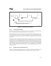
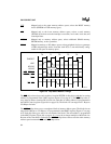
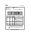
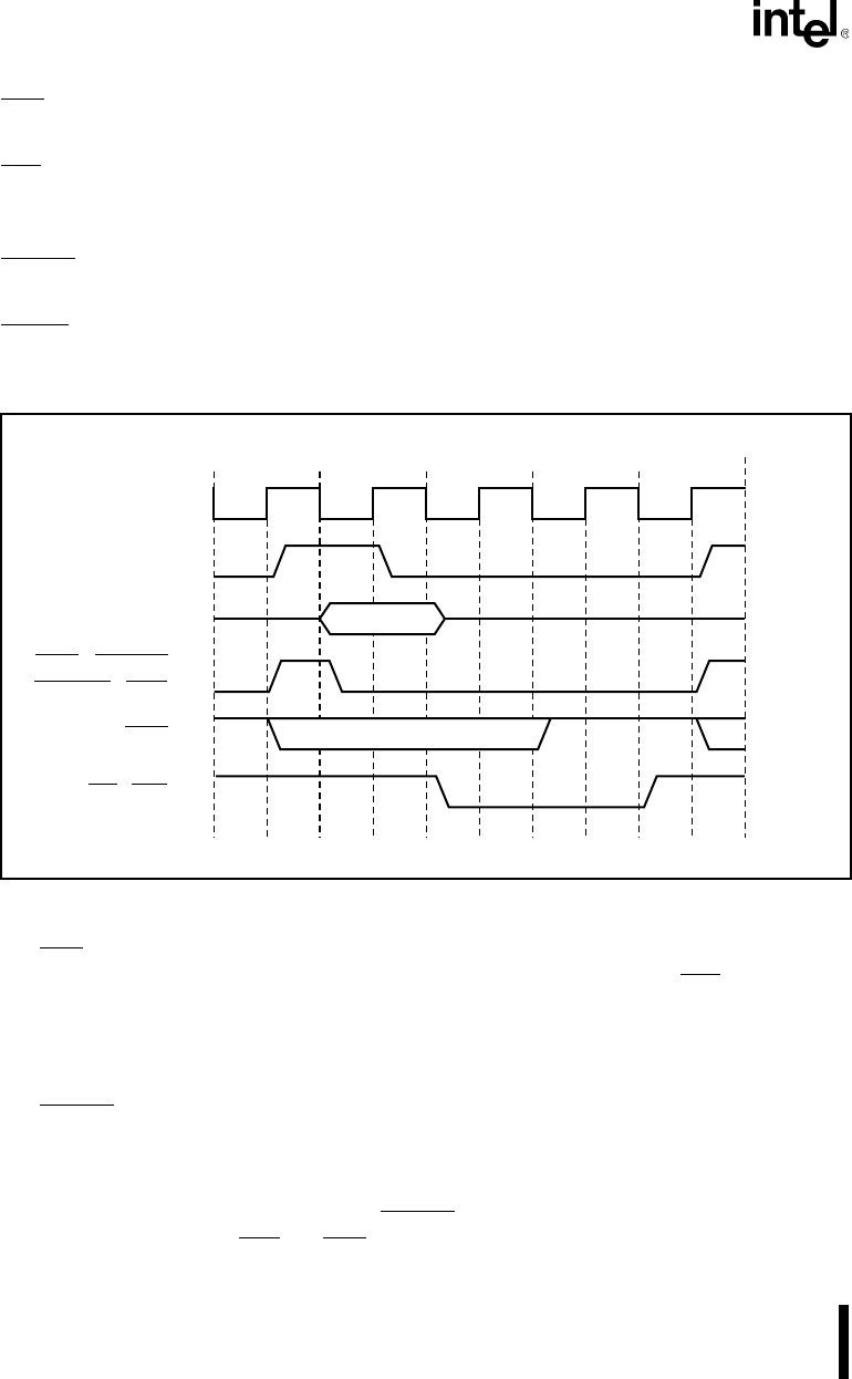
Figure 6-3. Chip-Select Relative Timings
The UCS chip-select always ends at address location 0FFFFH; its block size (and thus its starting
address) is programmed in the UMCS register (Figure 6-5 on page 6-7). The LCS
chip-select al-
ways starts at address location 0H; its block size (and thus its ending address) is programmed in
the LMCS Control register (Figure 6-6 on page 6-8). The block size can range from 1 Kbyte to
256 Kbytes for both.
The MCS3:0
chip-selects access a contiguous block of memory address space. The block size can
range from 8 Kbytes to 512 Kbytes; it is programmed in the MMCS register (Figure 6-7 on page
6-9). Each chip-select goes active for one-fourth of the block. The start address is programmed
in the MPCS register (Figure 6-9 on page 6-11); it must be an integer multiple of the block size.
Because of the start address limitation, the MCS3:0
chip-selects cannot cover the entire memory
address space between the LCS
and UCS chip-selects.
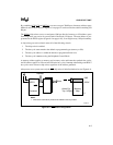
ALE
CLKOUT
T4 T1 T2 T3
AD15:0
A19:16
RD, WR
UCS, PCS6:0
MCS3:0, LCS
T4
S2:0
Status
Address Valid
A1140-0A