


3-25
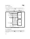
BUS INTERFACE UNIT
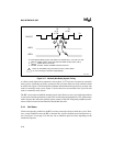
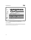
The minimum device data hold time (from WR high) is defined by T
DH
. The calculated value
must be greater than the minimum device requirements; however, the value can be changed only
by decreasing the clock rate.
T
WC
and T
WP
define the minimum time (maximum frequency) a device can process write bus cy-
cles. T
WR
determines the minimum time from the end of the current write cycle to the start of the
next write cycle. All three parameters require that calculated values be greater than device re-
quirements. The calculated T
WC
and T
WP
values increase with the insertion of wait states. The cal-
culated T
WR
value, however, can be changed only by decreasing the clock rate.
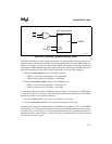
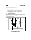
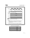
3.5.3 Interrupt Acknowledge Bus Cycle
Interrupt expansion is accomplished by interfacing the Interrupt Control Unit with a peripheral
device such as the 82C59A Programmable Interrupt Controller. (See Chapter 8, “Interrupt Con-
trol Unit,” for more information.) The BIU controls the bus cycles required to fetch vector infor-
mation from the peripheral device, then passes the information to the CPU. These bus cycles,
collectively known as Interrupt Acknowledge bus cycles, operate similarly to read bus cycles.
However, instead of generating RD
to enable the peripheral, the INTA signal is used. Figure 3-23
illustrates a typical Interrupt Acknowledge (or INTA
) bus cycle.
An Interrupt Acknowledge bus cycle consists of two consecutive bus cycles. LOCK
is generated
to indicate the sequential bus operation. The second bus cycle strobes vector information only
from the lower half of the bus (D7:0). In a 16-bit bus system, the upper half of the bus (D15:8)
floats.
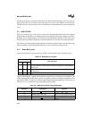
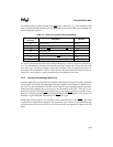
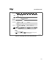
Table 3-5. Write Cycle Critical Timing Parameters
Memory Device
Parameter
Description Equation
T
WC
Write cycle time 4T
CLCL
T
AW
Address valid to end of write strobe (WR high) 3T
CLCL
–
T
ADLTCH
T
CW
Chip enable (LCS) to end of write strobe (WR high) 3T
CLCL
T
WR
Write recover time T
WHLH
T
DW
Data valid to write strobe (WR high) 2T
CLCL
T
DH
Data hold from write strobe (WR high) T
WHDX
T
WP
Write pulse width T
WLWH