


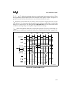
3-21
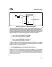
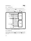
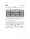
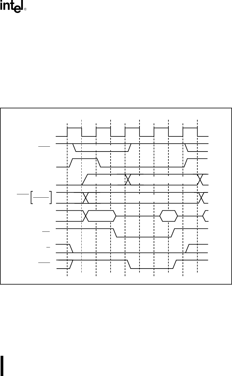
BUS INTERFACE UNIT
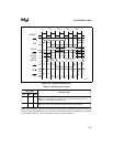
T
OE
, T
ACC
and T
CE
define the maximum data access requirements for the memory device. These
device parameters must be less than the value calculated in the equation column. An equal to or
greater than result indicates that wait states must be inserted into the bus cycle.
T
DF
determines the maximum time the memory device can float its outputs before the next bus
cycle begins. A T
DF
value greater than the equation result indicates a buffer fight. A buffer fight
means two (or more) devices are driving the bus at the same time. This can lead to short circuit
conditions, resulting in large current spikes and possible device damage.
T
RHAX
cannot be lengthened (other than by slowing the clock rate). To resolve a buffer fight con-
dition, choose a faster device or buffer the AD bus (see “Buffering the Data Bus” on page 3-34).
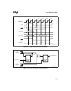
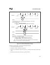
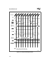
Figure 3-19. Typical Read Bus Cycle
ALE
S2:0
A19:16
CLKOUT
T1 T2 T3 T4
A18:16 = 0, A19=Valid Status
A15:8
RFSH
Valid
A15:0
[AD7:0]
RD
DT/R
DEN
BHE
Status Valid
Address Valid
Data
Valid
Address
Valid
A1046-0A