


TIMER/COUNTER UNIT
9-16
The input pins for Timers 0 and 1 provide an alternate method for enabling and disabling timer
counting. When using internal clocking, the input pin can be programmed either to enable the tim-
er or to reset the timer count, depending on the state of the Retrigger (RTG) bit in the control reg-
ister. When used as an enable function, the input pin either allows (input high) or prevents (input
low) timer counting. To ensure recognition of an input level, it must be valid for four CPU clocks.
This is due to the counter element’s time-multiplexed servicing scheme for the timers.
9.2.6 Timer Interrupts
All timers can generate internal interrupt requests. Although all three timers share a single inter-
rupt request to the CPU, each has its own vector location and internal priority. Timer 0 has the
highest interrupt priority and Timer 2 has the lowest.
Timer Interrupts are enabled or disabled by the Interrupt (INT) bit in the Timer Control register.
If enabled, an interrupt is generated every time a maximum count value is reached. In dual max-
imum count mode, an interrupt is generated each time the value in Maxcount Compare A or Max-
count Compare B is reached. If the interrupt is disabled after a request has been generated, but
before a pending interrupt is serviced, the interrupt request remains active (the Interrupt Control-
ler latches the request). If a timer generates a second interrupt request before the CPU services
the first interrupt request, the first request is lost.
9.2.7 Programming Considerations
Timer registers can be read or written whether the timer is operating or not. Since processor ac-
cesses to timer registers are synchronized with counter element accesses, a half-modified count
register will never be read.
When Timer 0 and Timer 1 use an internal clock source, the input pin must be high to enable
counting.
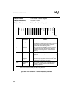
9.3 TIMING
Certain timing considerations need to be made with the Timer/Counter Unit. These include input
setup and hold times, synchronization and operating frequency.
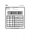
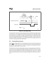
9.3.1 Input Setup and Hold Timings
To ensure recognition, setup and hold times must be met with respect to CPU clock edges. The
timer input signal must be valid T
CHIS
before the rising edge of CLKOUT and must remain valid
T
CHIH
after the same rising edge. If these timing requirements are not met, the input will not be
recognized until the next clock edge.