


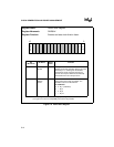
5-7
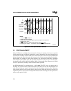
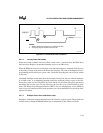
CLOCK GENERATION AND POWER MANAGEMENT
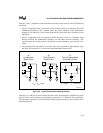
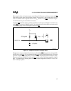
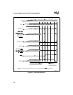
Reset may be either cold (power-up) or warm. Figure 5-6 illustrates a cold reset. Assert the RES
input during power supply and oscillator startup. The processor’s pins assume their reset pin
states a maximum of 28 X1 periods after X1 and V
CC
stabilize. Assert RES 4 additional X1 peri-
ods after the device pins assume their reset states.
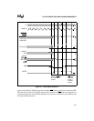
Applying RES
when the device is running constitutes a warm reset (see Figure 5-7). In this case,
assert RES
for at least 4 CLKOUT periods. The device pins will assume their reset states on the
second falling edge of X1 following the assertion of RES
.
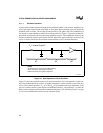
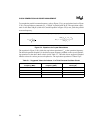
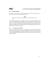
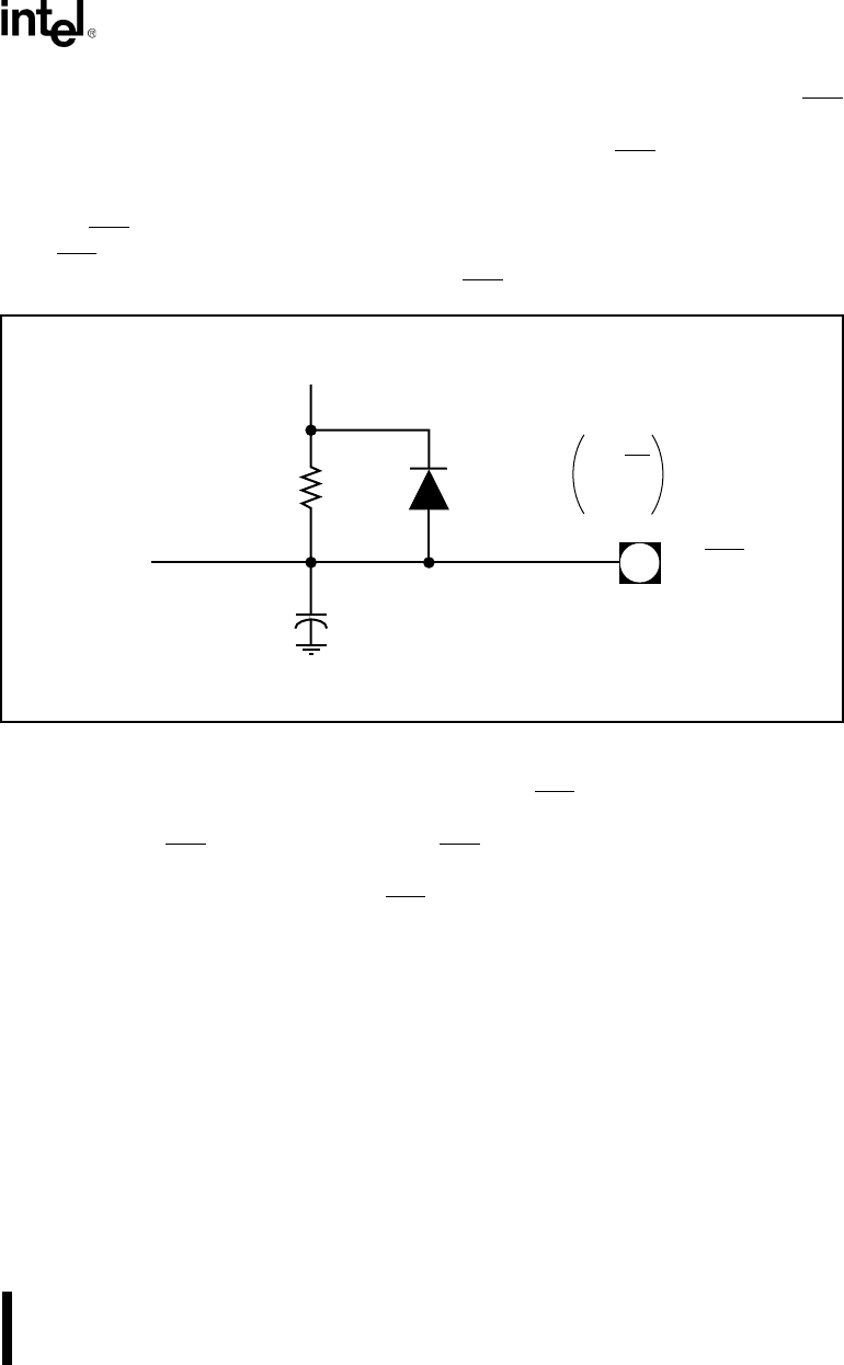
Figure 5-5. Simple RC Circuit for Powerup Reset
The processor exits reset identically in both cases. The falling RES edge generates an internal RE-
SYNC pulse (see Figure 5-8), resynchronizing the divide-by-two internal phase clock. The clock
generator samples RES
on the falling X1 edge. If RES is sampled high while CLKOUT is high,
the processor forces CLKOUT low for the next two X1 cycles. The clock essentially “skips a
beat” to synchronize the internal phases. If RES
is sampled high while CLKOUT is low, CLK-
OUT is already in phase.
RESET IN RES
1µf typical
50 k typical V = V
c(t)
V
cc
1 - e
-t
RC
A1521-0A