


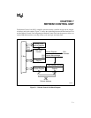
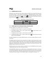

REFRESH CONTROL UNIT
7-8
7.7.2.1 Refresh Base Address Register
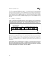
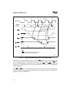
The Refresh Base Address Register (Figure 7-6) programs the base (upper seven bits) of the re-
fresh address. Seven-bit mapping places the refresh address at any 4 Kbyte boundary within the
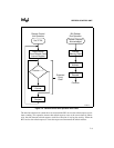
1 Mbyte address space. When the partial refresh address from the 9-bit address counter (see Fig-
ure 7-1 and “Refresh Control Unit Capabilities” on page 7-2) passes 1FFH, the Refresh Control
Unit does not increment the refresh base address. Setting the base address ensures that the address
driven during a refresh bus cycle activates the DRAM chip select.
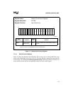
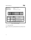
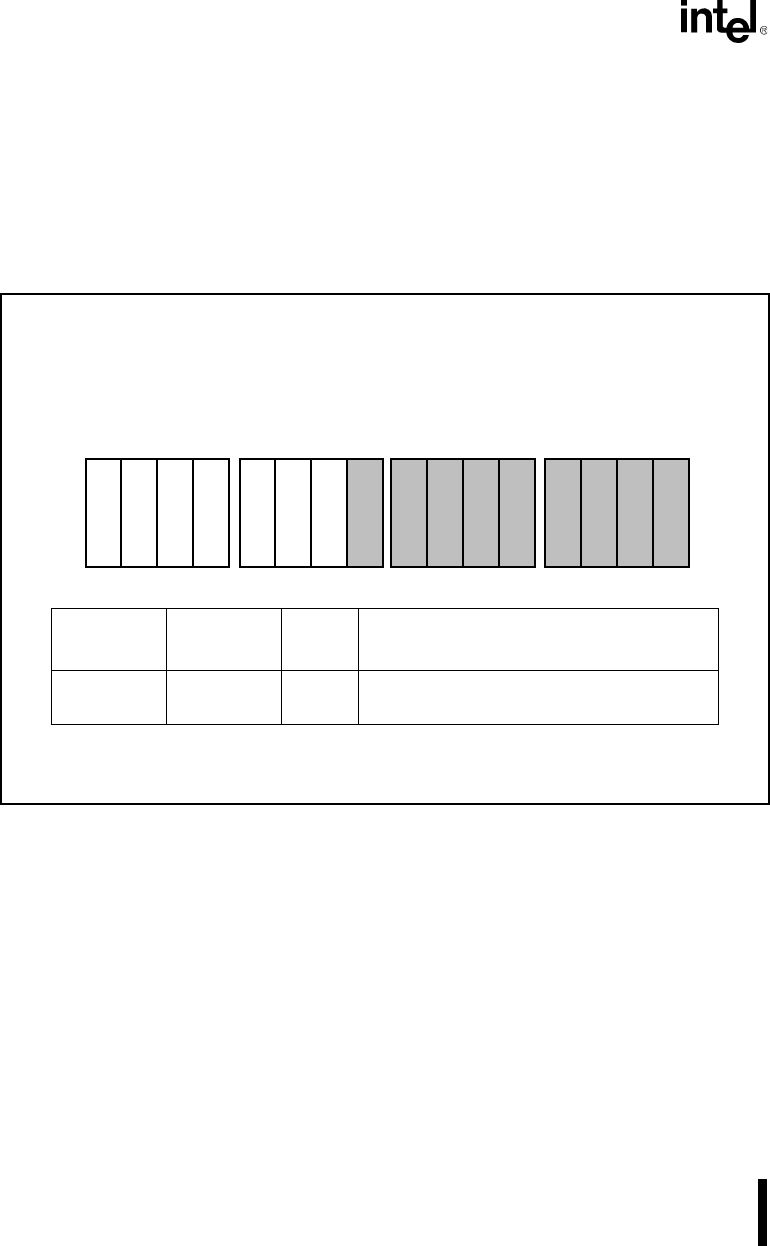
Figure 7-6. Refresh Base Address Register
7.7.2.2 Refresh Clock Interval Register
The Refresh Clock Interval Register (Figure 7-7) defines the time between refresh requests. The
higher the value, the longer the time between requests. The down-counter decrements every fall-
ing CLKOUT edge, regardless of core activity. When the counter reaches one, the Refresh Con-
trol Unit generates a refresh request, and the counter reloads the value from the register. Since
Power-Save mode divides the clock to the Refresh Control Unit, this register will require repro-
gramming if Power-Save mode is used.
Register Name: Refresh Base Address Register
Register Mnemonic: RFBASE
Register Function: Determines upper 7 bits of refresh address.
Bit
Mnemonic
Bit Name
Reset
State
Function
RA19:13 Refresh
Base
00H Uppermost address bits for DRAM refresh
cycles.
NOTE: Reserved register bits are shown with gray shading. Reserved bits must be written
to a logic zero to ensure compatibility with future Intel products.
15 0
R
A
1
3
R
A
1
4
R
A
1
5
R
A
1
6
R
A
1
7
R
A
1
8
R
A
1
9
A1503-0A