


3-23
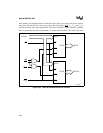
BUS INTERFACE UNIT
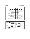
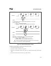
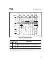
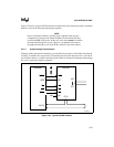
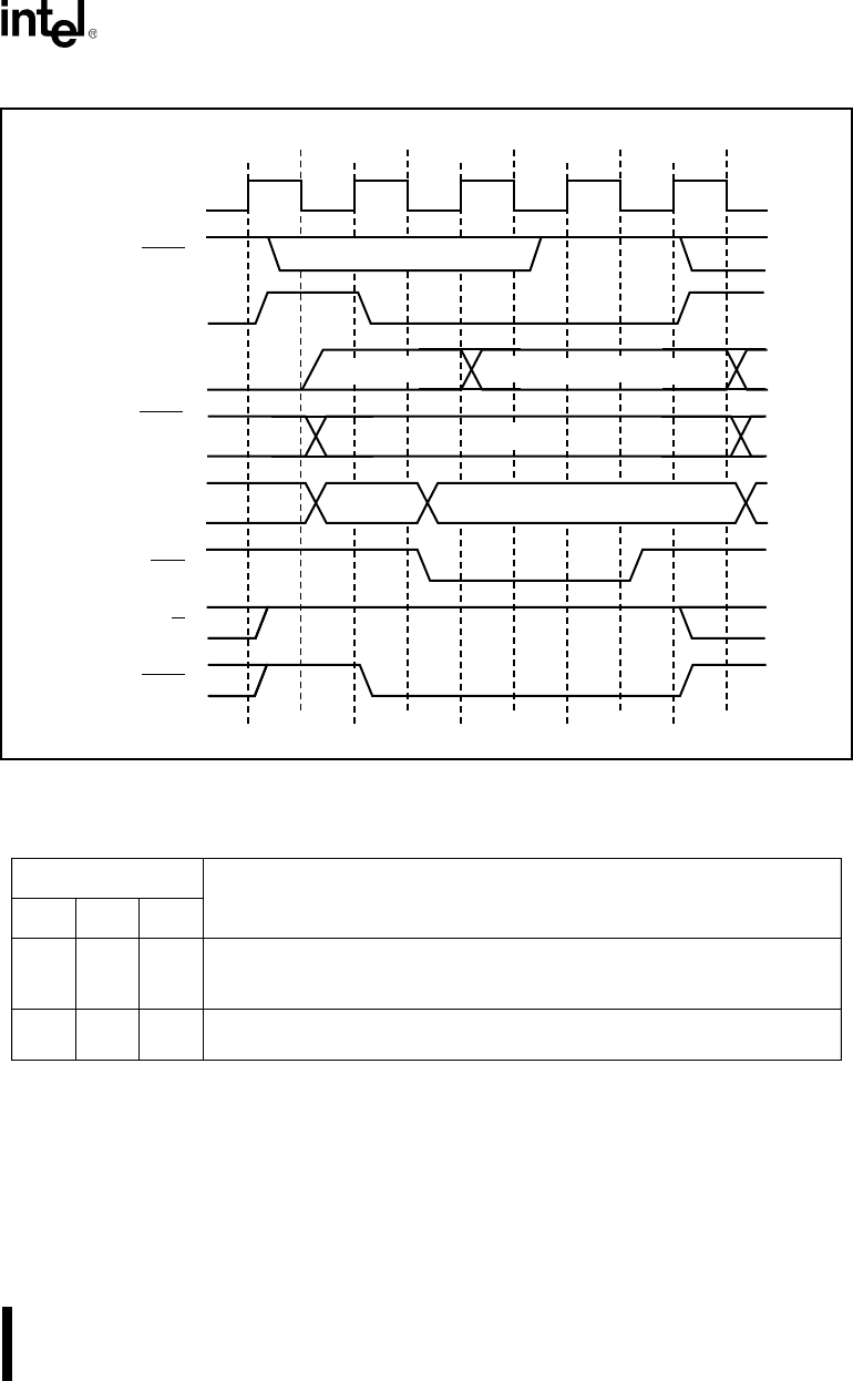
Figure 3-21. Typical Write Bus Cycle
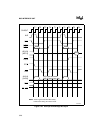
Figure 3-22 illustrates a typical 16-bit interface connection to a read/write device. Write bus cy-
cles have many parameters that must be evaluated in determining the compatibility of a memory
(or I/O) device. Table 3-5 lists some critical write bus cycle parameters.
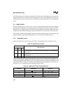
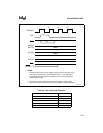
Table 3-4. Write Bus Cycle Types
Status Bits
Bus Cycle Type
S2 S1 S0
0 1 0 Write I/O — Initiated by executing IN, OUT, INS, OUTS instructions or by the
DMA Unit. A15:0 select the desired I/O port. A19:16 are driven to zero (see
Chapter 10, “Direct Memory Access Unit”).
1 1 0 Write Memory —Initiated by any of the Byte/ Word memory instructions or the
DMA Unit. A19:0 selects the desired byte or word memory location.
ALE
S2:0
A19:16
CLKOUT
T1 T2 T3 T4
A18:16 = 0, A19=Valid Status
Valid
A15:0
[AD7:0]
WR
DT/R
DEN
BHE
[A15:8]
Status Valid
Address Valid
Address
Valid
Data Valid
A1047-0A