


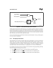
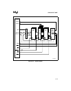

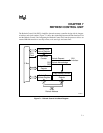

CHIP-SELECT UNIT
6-20
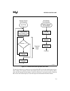
Example 6-1. Initializing the Chip-Select Unit
$ TITLE (Chip-Select Unit Initialization)
$ MOD186XREF
NAME CSU_EXAMPLE_1
; External reference from this module
$ include(PCBMAP.INC ;File declares register
;locations and names.
; Module equates
; Configuration equates
INTRDY EQU 0004H ;Internal bus ready modifier
EXTRDY EQU 0000H ;External bus ready modifier
IO EQU 0080H ;PCS Memory/IO select modifier
ALLPCS EQU 0040H ;PCS/Latched address modifier
;Below is a list of the default system memory and I/O environment. These
;defaults configure the Chip-Select Unit for proper system operation.
;EPROM memory is located from 0E0000 to 0FFFFF (128 Kbytes).
;Wait states are calculated assuming 16MHz operation.
;UCS# controls the accesses to EPROM memory space.
EPROM_SIZE EQU 128 ;Size in Kbytes
EPROM_BASE EQU 1024 - EPROM_SIZE;Start address in Kbytes
EPROM_WAIT EQU 1 ;Wait states
;The UMCS register values are calculated using the above system contraints
;and the equations below.
UMCS_VAL EQU (EPROM_BASE SHL 6)OR (0C038H) OR
& (EPROM_RDY) OR (EPROM_WAIT)
;SRAM memory starts at 0H and continues to 7FFFH (32 Kbytes).
;Wait states are calculated assuming 16MHz operation.
;LCS# controls the accesses to SRAM memory space.
SRAM_SIZE EQU 32 ;Size in Kbytes
SRAM_BASE EQU 0 ;Start address in Kbytes
SRAM_WAIT EQU 0 ;Wait states
SRAM_RDY EQU INTRDY ;Ignore bus ready
;The LMCS register value is calculated using the above system constraints
;and the equations below
LMCS_VAL EQU ((SRAM_SIZE - 1)SHL6) OR (0038H) OR
& (SRAM_RDY) OR (SRAM_WAIT)
;A DRAM interface is selected by the MCS3:0 chip-selects. The BASE value
;defines the starting address of the DRAM window. The SIZE value (along with
;the BASE ;value) defines the ending address. Zero wait state performance
;is assumed. The Refresh Control Unit uses DRAM_BASE to properly configure
;refresh operation.