


BUS INTERFACE UNIT
3-22
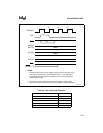
3.5.1.1 Refresh Bus Cycles
A refresh bus cycle operates similarly to a normal read bus cycle except for the following:
• For a 16-bit data bus, address bit A0 and BHE drive to a 1 (high) and the data value on the
bus is ignored.
• For an 8-bit data bus, address bit A0 drives to a 1 (high) and RFSH is driven active (low).
The data value on the bus is ignored. RFSH
has the same bus timing as BHE.
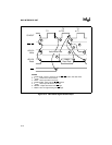
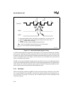
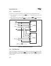
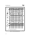
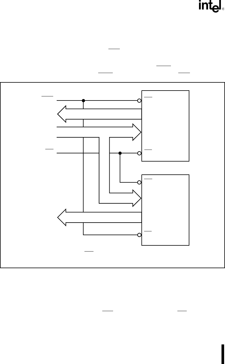
Figure 3-20. Read-Only Device Interface
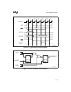
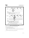
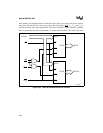
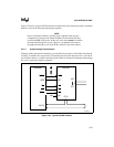
3.5.2 Write Bus Cycles
Figure 3-21 illustrates a typical write bus cycle. The bus cycle starts with the transition of ALE
high and the generation of valid status bits S2:0
. The bus cycle ends when WR transitions high
(inactive), although data remains valid for one additional clock. Table 3-4 lists the two types of
write bus cycles.
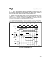
O
0-7
O
0-7
27C256
A
0-14
A
0-14
27C256
Note: A and BHE are not used.
0
UCS
RD
OE
OE
CE
CE
AD7:0
LA15:1
AD15:8
A1105-0A