


BUS INTERFACE UNIT
3-24
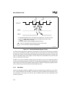
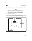
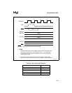
Most memory and peripheral devices latch data on the rising edge of the write strobe. Address,
chip-select and data must be valid (set up) prior to the rising edge of WR
. T
AW
, T
CW
and T
DW
de-
fine the minimum data setup requirements. The value calculated by their respective equations
must be greater than the device requirements. To increase the calculated value, insert wait states.
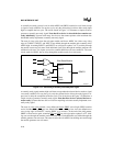
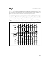
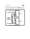
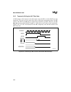
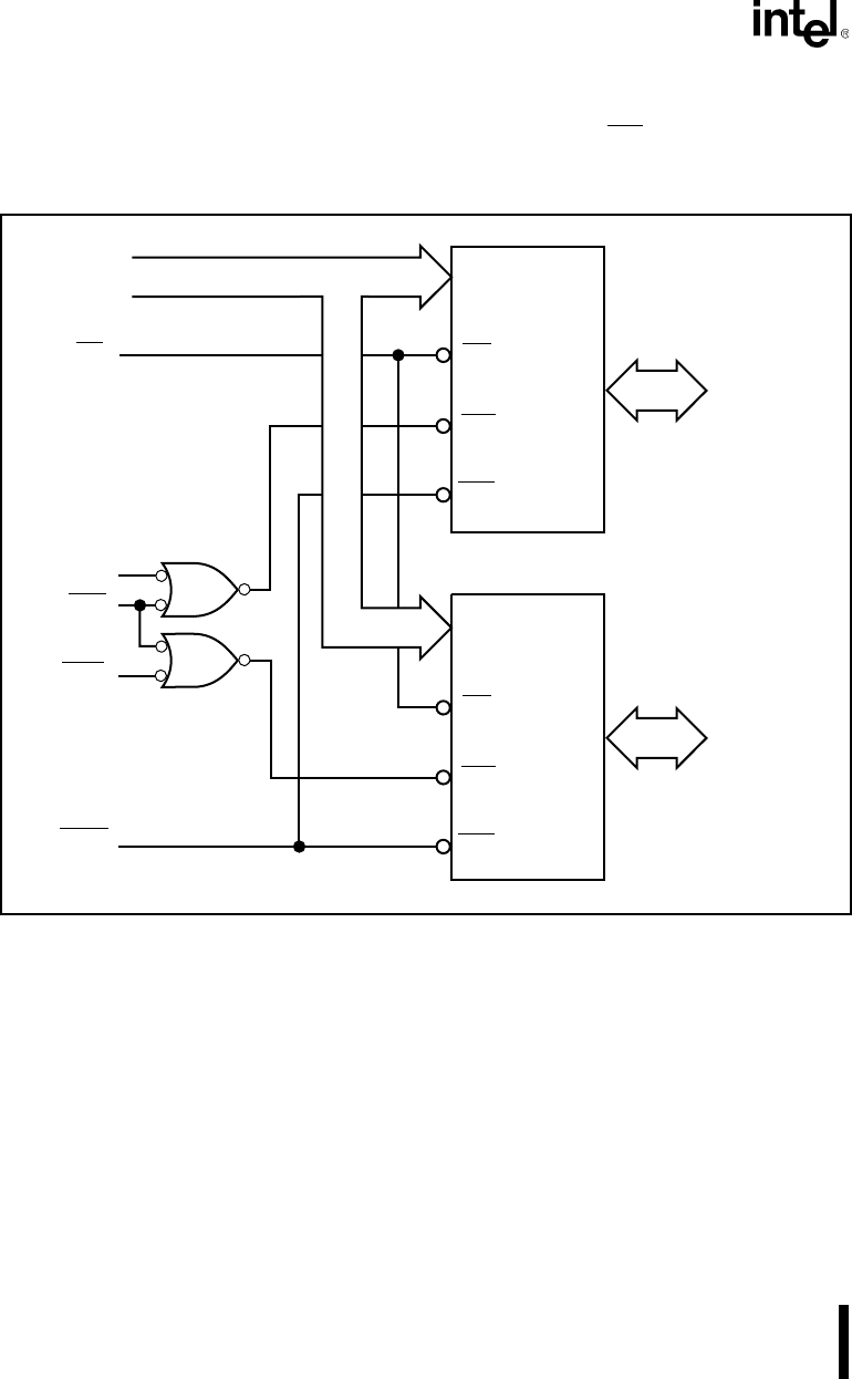
Figure 3-22. 16-Bit Bus Read/Write Device Interface
I/O1:8
A0:14
LA0
AD7:0
RD
OE
WE
CS1
WR
BHE
LCS
LA15:1
A0:14
OE
WE
CS1
I/O1:8
AD15:8
A1106-0A