


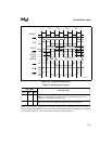
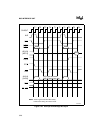
3-27
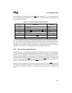
BUS INTERFACE UNIT
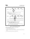
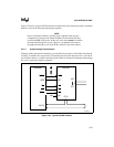
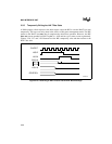
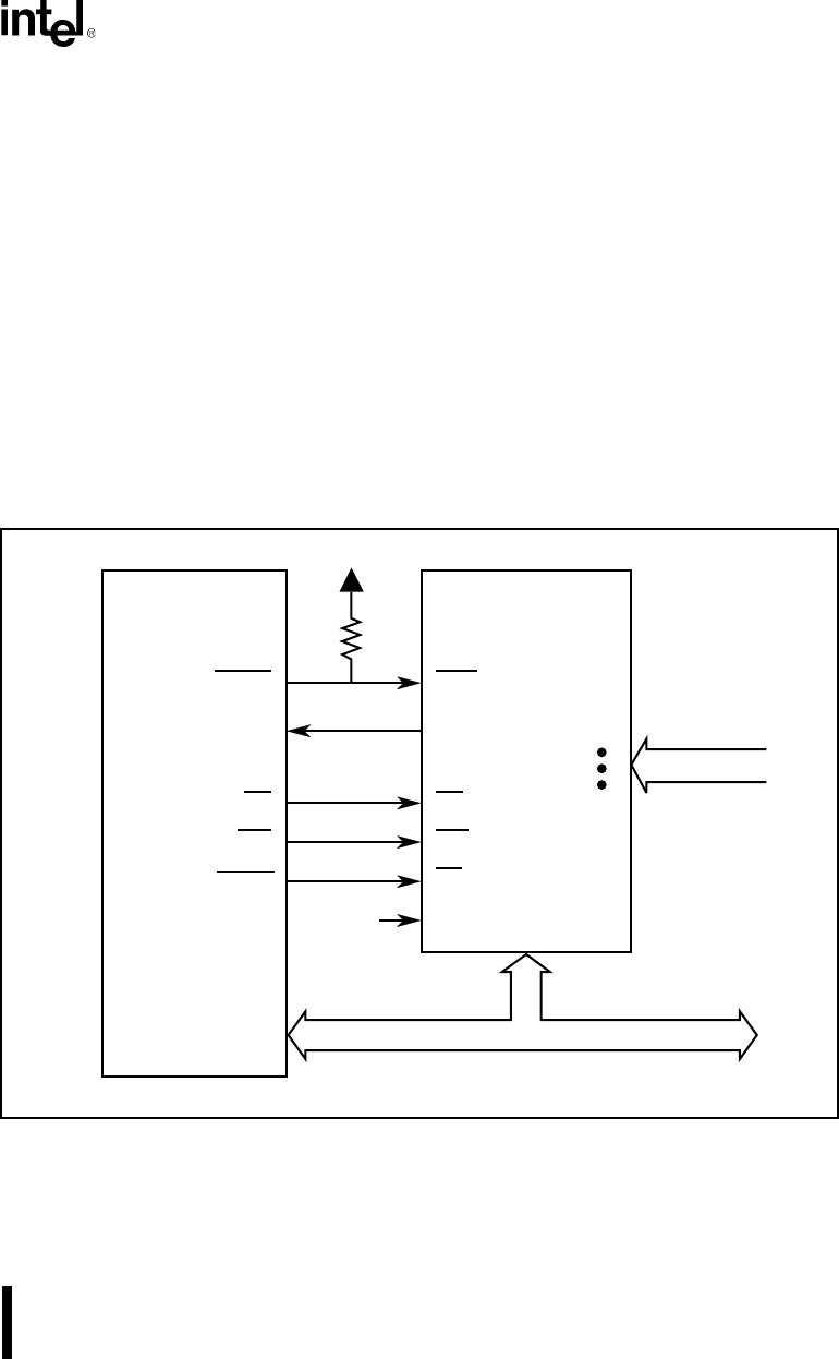
Figure 3-24 shows a typical 82C59A interface example. Bus ready must be provided to terminate
both bus cycles in the interrupt acknowledge sequence.
NOTE
Due to an internal condition, external ready is ignored if the device is
configured in Cascade mode and the Peripheral Control Block (PCB) is
located at 0000H in I/O space. In this case, wait states cannot be added to
interrupt acknowledge bus cycles. However, you can add wait states to
interrupt acknowledge cycles if the PCB is located at any other address.
3.5.3.1 System Design Considerations
Although ALE is generated for both bus cycles, the BIU does not drive valid address information.
Actually, all address bits except A19:16 float during the time ALE becomes active (on both 8-
and 16-bit bus devices). Address-decoding circuitry must be disabled for Interrupt Acknowledge
bus cycles to prevent erroneous operation.
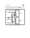
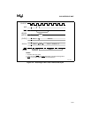
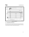
Figure 3-24. Typical 82C59A Interface
Processor
AD7:0
LA1
D7:0
A0
WR
IR0
IR7
82C59A
RD
GCS0
INTA
INT
INTA0
INT0
WR
RD
CS
A1065-0A
PCS0