


6-15
CHIP-SELECT UNIT
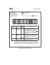
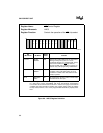
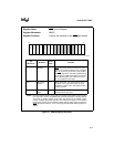
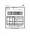
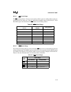
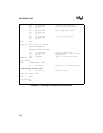
6.4.2.4 PCS Active Range
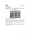
Each PCS chip-select starts at an offset above the base address programmed in the PACS register
and is active for 128 bytes. The base address can start on any 1 Kbyte memory or I/O address
location. Table 6-6 lists the active range for each PCS
chip-select.
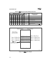
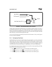
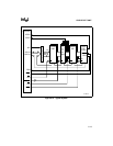
6.4.3 Bus Wait State and Ready Control
Normally, the bus ready input must be inactive at the appropriate time to insert wait states into
the bus cycle. The Chip-Select Unit can ignore the state of the bus ready input to extend and com-
plete the bus cycle automatically. Most memory and peripheral devices operate properly using
three or fewer wait states. However, accessing such devices as a dual-port memory, an expansion
bus interface, a system bus interface or remote peripheral devices can require more than three
wait states to complete a bus cycle.
A three-bit field (R2:0) in the control registers defines the number of wait states and the ready
requirements for the chip-selects. Figure 6-11 shows a simplified logic diagram of the wait state
and ready control functions.
Table 6-6. PCS Active Range
Chip-
Select
Active Range
Start Address Ending Address
PCS0
Base Base + 127 (7FH)
PCS1
Base + 128 (080H) Base + 255 (0FFH)
PCS2
Base + 256 (100H) Base + 383 (17FH)
PCS3
Base + 384 (180H) Base + 511 (1FFH)
PCS4
Base + 512 (200H) Base + 639 (27FH)
PCS5
Base + 640 (280H) Base + 767 (2FFH)
PCS6
Base + 768 (300H) Base + 895 (37FH)