


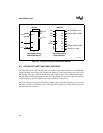
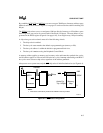
CHIP-SELECT UNIT
6-10
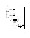
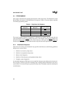
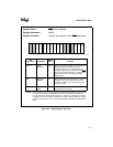
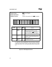
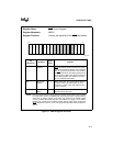
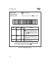
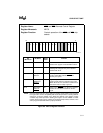
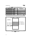
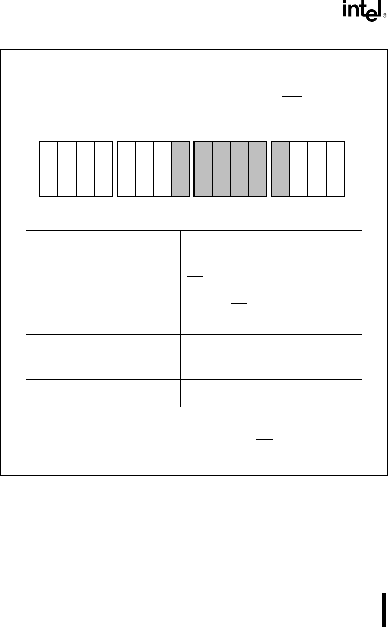
Figure 6-8. PACS Register Definition
Register Name: PCS Control Register
Register Mnemonic: PACS
Register Function: Controls the operation of the PCS
chip-selects.
Bit
Mnemonic
Bit Name
Reset
State
Function
U19:13 Start
Address
XXH Defines the starting address for the block of
PCS
chip-selects. During memory or I/O bus
cycles, U19:13 are compared with the A19:13
address bits. An equal to or greater than result
enables the PCS
chip-select. U19:16 must be
programmed to zero for proper I/O bus cycle
operation.
R2 Bus Ready
Disable
X When R2 is clear, bus ready must be active to
complete a bus cycle. When R2 is set, R1:0
control the number of bus wait states and bus
ready is ignored.
R1:0 Wait State
Value
3H R1:0 define the minimum number of wait states
inserted into the bus cycle.
NOTE: Reserved register bits are shown with gray shading. Reserved bits must be written
to a logic zero to ensure compatibility with future Intel products. U19:16 must be
programmed to zero for proper I/O bus cycle operation. Reading this register and
the MPCS register (before writing them) enables the PCS
chip-selects; however,
none of the programmable fields will be properly initialized.
15 0
R
1
R
0
R
2
U
1
3
U
1
5
U
1
4
U
1
7
U
1
6
U
1
9
U
1
8
A1143-0B